
2.1 Synchronous design in FPGA design
Asynchronous designs are not always able to meet the setup and hold time requirements of the triggers they feed. Therefore, asynchronous inputs often latch the wrong data to the flip-flop or put the trigger into a metastable state, in which the output of the flip-flop is not recognized as l or 0. Metastability can cause serious system reliability problems if not handled properly.
In addition, the most important part of the internal resources of the FPGA is its clock resource (global clock network), which usually enters the FPGA through the specific global clock pin of the FPGA, and then is adapted to the global clock network through the global clock BUF. Such a clock network can ensure that the difference in delay time for the same clock edge to reach each flip-flop inside the chip is negligible.
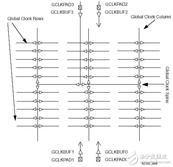
In the FPGA, the above-mentioned global clock network is called a clock tree. Whether it is a professional third-party tool or a layout router provided by a device manufacturer, the global clock network is used as a reference for calculation in delay parameter extraction and analysis. If a design does not use the clock provided by the clock tree, then some of these design tools will refuse to do delay analysis. Some delay data will be unreliable.
In many cases in our daily design, we need to use the frequency division. Many people use the high-frequency clock to count, and then use the output of the counter as the working clock for other logic design. In fact, this method is not standardized. For example, the following description method:
Process
Begin
Wait unTIl clk'event and clk='1';
If fck='1' then
Count<=(others=>'0');
Else
Count<=count+1;
End if;
End process;
Process
Begin
Wait unTIl count(2)'event and count(2)='1' ;
Shift_reg<=data;
End process;
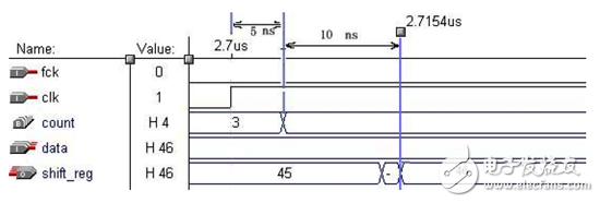
In the first process circuit description above, first, the output result of the counter (count(2)) has generated a certain delay with respect to the global clock clk (the magnitude of the delay depends on the number of bits of the counter and the selected use. Device process); while using the bit 2 of the counter as the clock in the second process, the delay of shift_reg relative to the global clk will become poorly controlled. The time analysis ultimately given by the place and route router is also unreliable. The result of this simulation is simulated as shown below:
The correct way to do this is to write the second process.
Process
Begin
Wait unTIl clk'event and clk='1' ;
If count(2 downto 0)=â€000†then
Shift_reg<=data;
End if;
End process;
Or write it in two steps:
Process(count)
Begin
If count(2 downto 0)=â€000†then
En<='1';
Else
En<='0';
End if;
End process;
Process
Begin
Wait unTIl clk'event and clk='1' ;
If en='1' then
Shift_reg<=data;
End if;
End process;
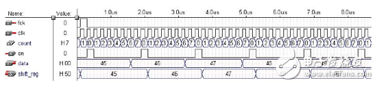
This is equivalent to generating an enable signal that is divided by eight, and the data data is sampled into the shift_reg register when the enable signal is valid. However, the delay of shift_reg in this case is relative to the global clock clk. The graphics below are more clearly visible.
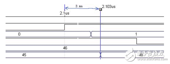
Partial magnification of the waveform in the above image
2.2 Generation of delay circuits in FPGA design:In the daily circuit design, sometimes we need to delay the signal to adapt to the timing relationship of the external interface. The most common and most typical case is the interface of the processor; because the timing relationship with the processed interface is asynchronous, And a standard FPGA design should be as synchronous as possible. So how do you deal with this situation?
First, a delay is generated in the FPGA, and the signal must pass through certain physical resources. There is a keyword Wait for xx ns in the hardware description language. It should be noted that the syntax is only used for simulation and cannot be used for synthesis. The comprehensive delay methods are:
Pass the signal through the logic gate to get a delay (if the door is not)
Use the delay unit provided by the device (such as Xilinx);
Note: Synthesizers tend to optimize when using multi-level NOT gates, because the synthesizer will consider a signal not twice or itself.
It should be noted that the internal structure of the FPGA/CPLD is a standard macrocell. The figure below is a standard macrocell of the Xilinx Spartans II family of devices. Although the chip macrocells of different manufacturers have different structures, they are generally composed of some combinatorial logic plus one or two flip-flops. In practical applications, when the combinatorial logic in a module is used, the corresponding flip-flop cannot be used; if the trigger unit is used, the combinatorial logic unit is also invalid. This is sometimes the case (especially with CPLDs). Although the design uses few resources, the place router reports the lack of resources.
Asia-Pacific generated the highest revenue in the market in 2017, and is expected to lead the global Lithium Iron Phosphate Battery market throughout the forecast period. The increasing demand for electric vehicles in the region is expected to drive the growth of Lithium Iron Phosphate batteries in this region. The growing use of Lithium Iron Phosphate batteries in renewable energy storage systems also accelerates the adoption. The increasing demand for consumer electronics from countries such as China, Japan, and India, along with stringent government regulations boost the Lithium Iron Phosphate Battery market growth.
The companies operating in the Lithium Iron Phosphate Battery market include Panasonic Corporation, Toshiba Corporation, Samsung SDI Co., Ltd, Toshiba Corporation, BYD Company Ltd., GS Yuasa Corporation, Valence Technology, Inc., A123 Systems, LLC., Formosa Energy & Material Technology, and Bharat Power Solutions. These companies launch new products and collaborate with other market leaders to innovate and launch new products to meet the increasing needs and requirements of consumers.
Portable Energy Storage System,Portable Energy Storage Market,Portable Power Storage,Portable Energy Storage
Shenzhen Sunbeam New Energy Co., Ltd , https://www.sunbeambattery.com