
Traditional solutions using depletion-mode FETs have wide variability in current and temperature coefficient. Figure 1 shows a two-terminal current source with two transistors and two Zener diodes. It provides acceptable current at both ends, but only a few percent accuracy. This circuit works in open loop, so it cannot provide the accuracy of a closed loop feedback circuit. Because the temperature coefficient of the Zener diode does not match the transistor well, the circuit will exhibit drift and errors based on the change in the base-emitter voltage VBE of the Zener diode and the transistor. In addition, a minimum voltage of approximately 3V is required across the circuit to function properly. Zener diodes (actually an IC) such as the LT1004 reduce the minimum operating voltage.
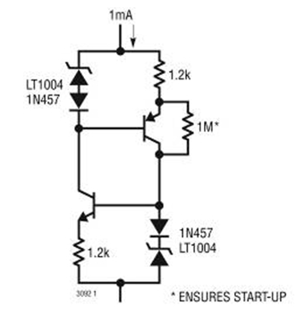
Figure 1: Current source at both ends.
The LT3092 overcomes a series of problems with traditional current sources at both ends and adds a versatile option for designers. By using a unit or parallel unit, the current source can provide a current value as low as 1mA. The regulation of voltage, load and temperature is quite good. The unique design method allows the device to work without bypass capacitor even if there is a complex feedback circuit inside the device.
LT3092 has good initial accuracy and very low temperature coefficient. The output current can be set in the range of 0.5mA to 200mA. The typical value of current regulation is 10ppm / V. The LT3092 operates at as low as 1.5V or as high as 40V. It provides 100MΩ impedance at 1mA and 1MΩ at 100mA. Unlike most other analog ICs, special design techniques have been used to achieve stable operation without power supply bypass capacitors, allowing it to provide high AC impedance and high DC impedance.
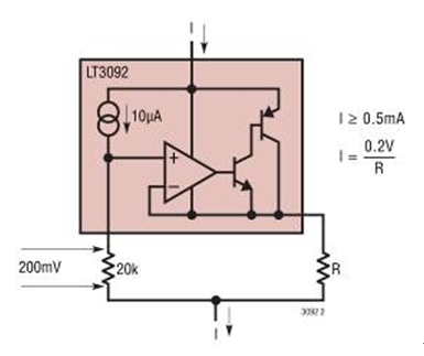
Figure 2: Current source across the LT3092.
Figure 2 shows the basic block diagram of the LT3092 current regulator. Its architecture is very similar to the LT3080 regulator, but it uses a PNP transistor as the output circuit. The internal circuit is differential and buffered, with a regulator to isolate it from power supply changes. This isolation allows stable operation without bypass capacitors. In addition, as far as the environment in which the power supply can be reversed, the LT3092 can avoid damage caused by reverse power supply voltage, and does not conduct current, thereby protecting the load.
The internal current source and amplifier offset are to achieve 100dB or better power supply variation suppression, so its regulation performance is very good. Lowering RSET to 0Ω will also lower the output to 0V.
A small voltage is applied to an external setting resistor of 20kΩ to produce a 200mV reference. This makes the voltage across the resistor R that determines the current 200mV, then the total current is equal to 0.2V divided by R (10μA). The current stabilizer works when the voltage between the two ends is about 1.5V to 36V, and the current stability and temperature stability are excellent. As a current source at both ends, its load can be in the forward branch of the circuit or in the branch to ground.
The 200mV reference voltage will compensate for errors due to changes in the internal current source and amplifier offset as the power supply voltage changes. As the power supply changes, the internal current source changes by about 50pA / V. The variation of the internal operational amplifier offset is less than 5μV / V. Assuming that the current source and amplifier offsets are the worst case, using a 200mV reference makes the amplifier and internal current source pair produce the same error. If you increase the 200mV to 500mV by using a 50kΩ resistor, the offset of the internal operational amplifier will be reduced. This improves the stability of the current source relative to power supply changes. However, the regulation of the loop is quite good. In general, the voltage across the resistor is set in the range of 100mV to 200mV.
Setting the resistance also allows the burden of trimming the total current to be reduced. If this circuit is used in the case of a large current of 100mA, since the value of the resistance R is very small, it is difficult to fine-tune the current. However, the 20k resistor is always very easy to adjust to set the current value to the desired level. Figure 3 shows the start-up time, while Figure 4 shows the change in current source with temperature at a 1mA output current value.
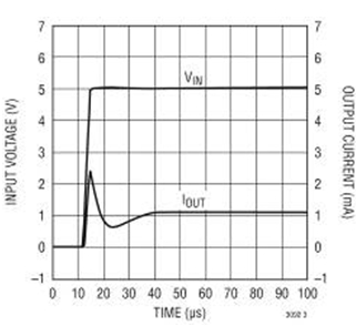
Figure 3: The startup time to reach 1mA is less than 20μs.
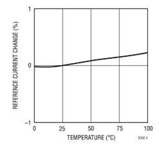
Figure 4: Reference current changes with temperature.
Improve voltage consistency
For higher voltages, current sources can be superimposed to work at higher total voltages. Figure 5 shows the superimposed current source.
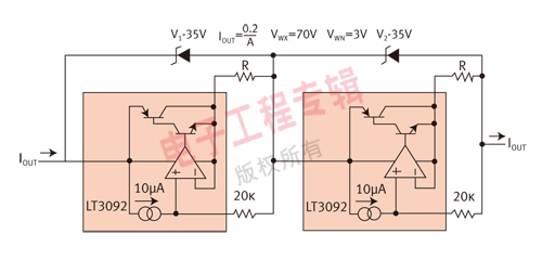
Figure 5: Current sources are superimposed to achieve a higher operating voltage.
Two current sources are set up for the same current, and a voltage-limiting zener diode is placed across each current source. Under low voltage conditions, the current source that increases faster will saturate, and the current will now be controlled by another current source. When the voltage gradually increases, the Zener diode will be activated and begin to conduct current. Then, the voltage across the saturation current source begins to increase. Moreover, it will regulate the current as the voltage continues to increase. When current control moves from one current source to another, the discontinuity in the output current is equivalent to the error between the two current sources. This is usually less than 1%, and also bypass capacitors are not required to make the device work properly.
In terms of large setting current and high voltage, the power consumption of the LT3092 is quite large. For example, 30V and 100mA is equivalent to 3W power consumption, depending on the thermal resistance of the PC board, which may cause the temperature to rise greatly. An external resistor can transfer part of the power to it and reduce the power consumption in the LT3092. Figure 6 shows the basic current source with a resistor RX from the input to the output of the device. As long as the total current is higher than the current through RX, it will not affect the steady state, and the impedance of the current source will not change. The current through RX is in the feedback loop and is compensated as the voltage changes from input to output. This current flows through an internal PNP transistor or external resistor, and the feedback loop keeps the total current constant.
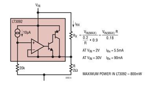
Figure 6: 100mA current source with power transfer resistor.
In order to achieve good regulation and reasonable margin, as far as the device is at maximum voltage, the current through RX should not be greater than 90% of the required current. The formula in the figure shows how to select RX so that the current flowing through RX is always at least 10% of the current flowing through LT3092. By transferring some power to an external resistor, the maximum internal power is reduced. This greatly reduces the power consumption in the device and reduces the temperature rise. The introduction of this external resistance has little effect on the performance of the circuit.
If a larger output current is required, the current sources can be directly connected in parallel. You can use two LT3092s (with or without power transfer resistors) and directly connect them in parallel to get twice the output current. Figure 7 shows a 300mA current source operating at both ends.
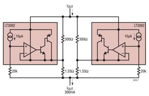
Figure 7: Parallel current source with power transfer resistor.
Figure 8 shows another method of paralleling devices. Because it requires fewer external components, it may be a better way to parallel multiple devices to obtain high current. In this case, the setting pins are connected together, which makes the output pins of the ballast differ from each other within a few millivolts. Then, the output of the current stabilizer is the sum of the steady current resistance flowing through 40mΩ, so as to achieve current sharing. These resistors are usually arranged on a small PCB on which the device is mounted. Next, we increased the voltage drop from 200mV to 1V by using a 100kΩ setting resistor. This is to minimize the effect of the temperature coefficient on the stable current resistance of the printed circuit traces.
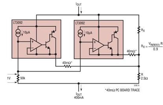
Figure 8: Parallel current sources to spread heat and achieve greater output current.
These steady current resistors made of copper wire have a voltage difference of about 8mV across the two ends. The temperature coefficient of the copper wire is 0.3% per degree, and this will affect the temperature coefficient of the entire current source. Increasing the reference voltage from 200mV to 1V will make the proportion of the voltage across the ballast resistor smaller, and for a temperature change of 100 ° C, this effect will be reduced from approximately 1% to 0.2%.
Increasing the output current to more than 400mA requires only an additional parallel device and a ballast resistor, so in terms of high current, this minimizes the number of devices. At high voltage, we shunt part of the current around the IC through RX to reduce device power consumption.
The current source can drive any type of load. Since the device is actually a complex integrated circuit, the load impedance may affect the internal circuit and cause some instability. Although great efforts have been made to make the device stable when driving various loads, instability may still exist.
It is actually easy to stabilize the device. A resistor can be inserted in series with the ballast, or a capacitor (basically a bypass capacitor) or RC can be connected across Vin and Vout of the device. This gives the device a known impedance, making it stable when it encounters an unknown impedance. Unlike older adjustment elements, the capacitor can be very small.
The harsh line environment with spike voltage, noise, or radio frequency will provide a bypass for noise and spikes, thereby protecting the internal circuit of the ballast. In terms of stability, capacitors as low as 1,000pF can be used. However, capacitors from 0.01 μF to 1 μF can also be used. It is worth noting that some ceramic capacitors have very high voltage coefficients that can change from 5 to 1 as the voltage changes.
The capacitor does not affect the impedance of the current source at low frequencies, because like the external resistor RX, it is also inside the feedback loop. In terms of the AC change across the device, current flows through the capacitor or the internal transistor of the LT3092, so the impedance does not change. At high frequencies, because the LT3092 operates outside the bandwidth, the impedance is capacitive relative to the LT3092.
For loads with large voltage changes during operation, the current through the capacitor must be lower than the programmed current. Otherwise, when the current higher than the programmed current passes through the capacitor, the loop will be damaged. The allowable voltage change rate of the device is shown in Figure 9, and still about 90% of the current flows through the capacitor without affecting the impedance of the LT3092 current source. For example, in the case of a 1mA load and a 1μF capacitor across the device, the circuit will allow a voltage change rate of 1000V / s. The capacitance, rate of change of voltage, and other effects of current can be calculated very easily.

Figure 9: Voltage change circuit.
The LT3092 can also act as a voltage regulator without an output capacitor. "Intrinsically safe" applications are often designed with low current and small capacitance (or no capacitor). Figure 10 shows a 200mA regulator. As a voltage regulator, the 10μA current generated inside the LT3092 will flow through an external RSET resistor. The voltage applied to the SET pin is the product of this 10μA current and RSET resistance. The internal voltage follower provides the same voltage at the output pin as the set pin. The load is connected from the output pin to ground.

Digital Accessories producs including Wireless Bluetooth Earphone, Mobile phone Wireless Charger, Mobile phone data cable, Mobile phone selfie holder and Mobile phone USB Disk, etc. They are all computer or mobile phone peripherals products. These kinds of products will bring more convenient when you use mobile phone, they are all real good partners of smart phone. Any inquirey please feel free to contact us and welcome you to visit our company.


Digital Accessories
Digital Accessories,Wireless Charger,USB Data Cable,Bluetooth Selfie Stic
Shenzhen New Wonderful Technology Co., Ltd. , https://www.sznewwonderful.com