
The high reliability of LEDs (lifetime over 50,000 hours), high efficiency ("120 lumens/watt" and near-instantaneous responsiveness make it an attractive source of light. Compared to the response time of an incandescent bulb of 200mS, the LED will illuminate in just 5nS response time. Therefore, they are currently widely used in brake lights in the automotive industry.
1 drive LED
Driving LEDs is not without challenges. The adjustable brightness requires a constant current to drive the LED and it must be kept constant regardless of the input voltage. This is more challenging than simply connecting an incandescent bulb to a battery to power it.
The LED has a forward VI characteristic similar to a diode. Below the LED turn-on threshold (the white LED's turn-on voltage threshold is approximately 3.5V), the current through the LED is very small. Above this threshold, the current will increase exponentially in the form of a forward voltage. This allows the LED to be shaped as a voltage source with a series resistor with a warning that the model is only valid at a single operating DC current. If the DC current in the LED changes, the resistance of the model should also change to reflect the new operating current. At large forward currents, power dissipation in the LEDs can cause the device to heat up, which will change the forward voltage drop and dynamic impedance. It is important to fully consider the thermal environment when determining the LED impedance.
When driving LEDs through a buck regulator, the LEDs often conduct the AC ripple current and DC current of the inductor based on the selected output filter arrangement. This not only increases the RMS amplitude of the current in the LED, but also increases its power consumption. This increases the junction temperature and has a significant impact on the life of the LED. If we set a 70% light output limit as the life of the LED, the LED's lifetime will extend from 15,000 hours at 74 degrees Celsius to 40,000 hours at 63 degrees Celsius. The power loss of the LED is determined by multiplying the LED resistance by the square of the RMS current plus the average current multiplied by the forward voltage drop. Since the junction temperature can be determined by the average power consumption, even a large ripple current has little effect on power consumption. For example, in a buck converter, the peak-to-peak ripple current equal to the DC output current (Ipk-pk = Iout) increases by no more than 10% of the total power loss. If you exceed the above loss level, you need to reduce the AC ripple current from the power supply to keep the junction temperature and operating life constant. A very useful rule of thumb is that for every 10 degrees Celsius reduction in junction temperature, semiconductor lifetime will be doubled. In fact, most designs tend to have lower ripple currents due to the suppression of the inductor. In addition, the peak current in the LED should not exceed the maximum safe operating current rating specified by the manufacturer.
2 LED drive power topology selection analysis
In LED lighting applications with AC-DC power supplies, the power conversion building blocks include discrete components such as diodes, switches (FETs), inductors and capacitors, and resistors to perform their functions, while pulse width modulation (PWM) regulators are used to control Power conversion. The isolated AC-DC power conversion with a transformer usually included in the circuit includes topologies such as flyback, forward and half bridge. See Figure 3, where the flyback topology is the standard choice for medium and low power applications with power less than 30 W. The half-bridge structure is best suited to provide higher energy efficiency/power density. For transformers in isolated structures, the size of the transformer is related to the switching frequency, and most isolated LED drivers basically use "electronic" transformers.

Figure 1: LLC Half-Bridge Resonant Topology
In LED lighting applications using DC-DC power supplies, LED drivers can be used in the form of resistors, linear regulators, and switching regulators. See Figure 4 for a basic application. In the resistive drive mode, the forward current of the LED can be controlled by adjusting the current sense resistor in series with the LED. This drive mode is easy to design, low in cost, and has no electromagnetic compatibility (EMC) problem. The disadvantage is that it depends on the voltage and needs to be filtered. (binning) LED with low energy efficiency. Linear regulators are also easy to design and have no EMC issues. They also support current regulation and fold back, and provide an external current set point. The power dissipation problem is insufficient, and the input voltage is always higher than the forward voltage. Voltage, and energy efficiency is not high. The switching regulator continuously controls the opening and closing of the switch (FET) through the PWM control module to control the flow of current.
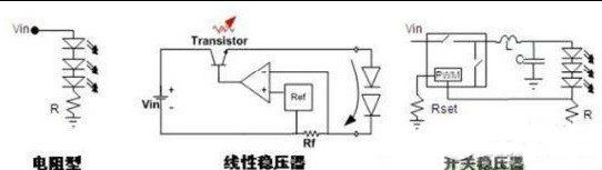
Figure 2: Common DC-DC LED Drivers
Switching regulators have higher energy efficiency, are independent of voltage, and can control brightness. Insufficient is relatively high cost, high complexity, and electromagnetic interference (EMI) problems. Common topologies for LED DC-DC switching regulators include Buck, Boost, Buck-Boost, or Single-Ended Primary Inductor Converter (SEPIC). Where the lowest input voltage under all operating conditions is greater than the maximum voltage of the LED string, a buck structure is used, such as driving 6 LEDs in series with 24 Vdc; in contrast, when the maximum input voltage is less than the minimum output voltage under all operating conditions Boost structure, such as 6 series LEDs driven by 12 Vdc; and the input voltage and output voltage range overlap can be buck-boost or SEPIC structure, such as 12 Vdc or 12 Vac to drive 4 series LEDs However, the cost and energy efficiency of this structure is the least desirable.
The way to directly drive LEDs with AC power has also achieved some development in recent years. See Figure 5 for the application diagram. In this configuration, the LED strings are arranged in opposite directions, operating in a half cycle, and the LEDs are turned on when the line voltage is greater than the forward voltage. This structure has its advantages, such as avoiding the power loss caused by AC-DC conversion. However, in this configuration, the LED is switched at a low frequency, so the human eye may be aware of flicker. In addition, LED protection is required in this design to protect it from line surges or transients.
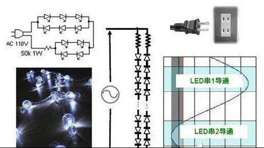
Figure 3: Schematic diagram of direct use of AC driven LEDs
3 LED topology selection example analysis
The information shown in Figure 4 helps to choose the best switching topology for the LED driver. In addition to these topologies, you can use simple current limiting resistors or linear regulators to drive LEDs, but such methods typically waste too much power. All relevant design parameters include input voltage range, number of LEDs driven, LED current, isolation, EMI suppression, and efficiency. Most LED driver circuits fall into the following topology types: buck, boost, buck-boost, SEPIC, and flyback.
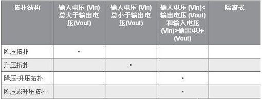
Figure 4: Alternative LED Power Topology
Figure 5 shows three basic power supply topology examples. The buck regulator shown in the first diagram is suitable for situations where the output voltage is always less than the input voltage. In Figure 5, the buck regulator controls the current into the LED by changing the turn-on time of the MOSFET. Current sensing can be obtained by measuring the voltage across the resistor, where the resistor should be in series with the LED. An important design challenge for this approach is how to drive the MOSFET. From a cost-effective point of view, it is recommended to use an N-channel field effect transistor (FET) that requires a floating gate drive. This requires a drive transformer or floating drive circuit (which can be used to maintain the internal voltage above the input voltage).
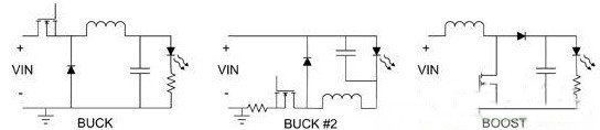
Figure 5: Simple Buck and Boost Topologies Power LEDs
Figure 5 also shows an alternative buck regulator (buck #2). In this circuit, the MOSFET drives the ground, which greatly reduces the driver circuit requirements. The circuit can choose to sense the LED current by monitoring the FET current or a current sense resistor in series with the LED. The latter requires a level shifting circuit to obtain information on the power ground, but this complicates the simple design. In addition, Figure 5 shows a boost converter that can be used when the output voltage is always greater than the input voltage. This topology is easy to design because the MOSFET is driven to ground and the current sense resistor is also grounded. One disadvantage of this circuit is that there is no limit to the current through the inductor during a short circuit. You can add fault protection in the form of a fuse or electronic circuit breaker. In addition, some of the more complex topologies provide this type of protection.

Figure 6: Buck-Boost Topology Adjusts Input Voltage Greater Than or Less Than Vout
Figure 6 shows two buck-boost circuits that can be used when the input voltage and output voltage are high and low. Both have the same trade-off characteristics (where the tradeoff can be seen in two buck topologies for current sense resistors and gate drive positions). The buck-boost topology in Figure 6 shows the gate drive for a ground reference. It requires a level shifted current sense signal, but the reverse buck-boost circuit has a ground referenced current sense and level shifted gate drive. If the control IC is associated with a negative output and the current sense resistor and LED are interchangeable, the reverse buck-boost circuit can be configured in a very useful manner. With proper control ICs, the output current can be measured directly and the MOSFET can be driven directly.
One drawback of this buck-boost method is that the current is quite high. For example, when the input and output voltages are the same, the inductor and power switch currents are twice the output current. This has a negative impact on efficiency and power consumption. In many cases, the “buck or boost†topology in Figure 7 will alleviate these problems. In this circuit, the buck power stage is followed by a boost. If the input voltage is higher than the output voltage, the buck stage will be voltage regulated when the boost stage is just energized. If the input voltage is less than the output voltage, the boost stage is regulated and the buck stage is powered. Some overlap is usually reserved for boost and buck operations, so there is no dead band when moving from one model to another.
When the input and output voltages are nearly equal, the benefit of this circuit is that the switching and inductor currents are also nearly identical to the output current. The inductor ripple current also tends to become smaller. Even with four power switches in the circuit, efficiency is typically significantly improved, which is critical in battery applications. The SEPIC topology is also shown in Figure 7, which requires fewer FETs but requires more passive components. The benefit is a simple ground reference FET driver and control circuitry. In addition, the dual inductors can be combined into a single coupled inductor, saving space and cost. But like a buck-boost topology, it has a higher switching current than the "buck or boost" and ripple output currents, which requires the capacitor to pass a larger RMS current.
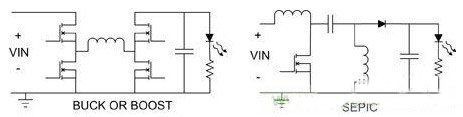
Figure 7: Buck or boost and SEPIC topologies provide greater efficiency
For safety reasons, it may be stipulated to use isolation between the off-line voltage and the output voltage. The most cost-effective solution for this application is the flyback converter (see Figure 8). It requires the least number of components in all isolated topologies. The transformer turns ratio can be designed as a buck, boost or buck-boost output voltage, which provides great design flexibility. But the downside is that the power transformer is usually a custom component. In addition, there is high component stress in the FET and in the input and output capacitors. In stable lighting applications, power factor correction (PFC) can be achieved by using a “slow†feedback control loop that adjusts the LED current in phase with the input voltage. A higher power factor is achieved by adjusting the average LED current required and the input current in phase with the input voltage.

Figure 8: Flyback converter provides isolation and power factor correction
4 dimming technology
It is quite common to need to dim the LEDs. For example, it may be necessary to adjust the display or adjust the brightness of the architectural light. There are two ways to do this: reduce the LED current or turn the LED on quickly and then turn it off, then let the eye eventually get balanced. Since the light output is not completely linear with the current, the method of reducing the current is the least efficient. In addition, LED chromatography typically changes when the current is below the rated value. Remember that people's perception of brightness is exponentially multiplied, so dimming requires a larger percentage change in current. Because at 3% of the full current, the 3% adjustment error can be amplified to 30% or more with a 10% load due to circuit tolerance, which can have a significant impact on circuit design. Although there is a problem with response speed, it is still more accurate to adjust the current by pulse width modulation (PWM). When lighting and displaying, PWM above 100Hz is required to make the human eye not notice the flicker. The 10% pulse width is in the millisecond range and requires a power supply with a bandwidth above 10 kHz.
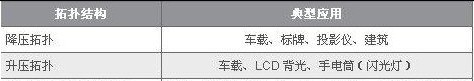
Figure 9: Many LED applications specify multiple power topologies
5 Conclusion
As shown in Figure 9, the use of LEDs in many applications is becoming increasingly common. It will use a variety of power topologies to support these applications. Typically, the input voltage, output voltage, and isolation requirements will dictate the correct choice. When the input voltage is always high and low compared to the output voltage, buck or boost may be the obvious choice. However, when the relationship between the input and output voltages is not so suppressed, the choice becomes more difficult, and many factors, including efficiency, cost, and reliability, need to be weighed.
Edit: Cedar
Prismatic Lithium Ion Battery is Rechargeable battery and extensively applied in mobile phone and cell phone for Nokia, Samsung and other brands. Its size and capacity also can be customized according to customer's requirements. It also has many merits: good safety performance, high energy density, excellent charge retention, long cycle life, low self-discharge rate, low resistance, no memory effect and non-pollution. Welcome to contact us for any battery need !
Lithium Ion Battery
Lithium Ion Battery,Small Lithium Ion Battery,Li Ion Battery,3.7V Lithium Ion Battery
Shenzhen Powercom Electronics Co., Ltd. , https://www.expowercome.com