
Abstract: Aiming at the requirements of the hardware platform required for the research of the latter three generations of mobile communication systems, a design scheme of scalable intermediate frequency receiver with strong flexibility is proposed. This scheme can realize the digital reception of signals at a higher intermediate frequency, and is suitable for a variety of input signals. Based on a top-down approach, this solution draws on the advantages of other solutions and completes the design of a digital receiver based on the idea of ​​software radio. The system is simple in structure, low in cost, and has good practicability and versatility.
In recent years, the development of mobile communication is very rapid. In response to the demand for higher-speed services, research on the latter three generations of mobile communication systems (B3G) has gradually emerged in China, but currently it is mostly limited to the theoretical research and simulation stage of simulation data. It is necessary to establish a hardware experiment platform in order to find research Method of application of results. This hardware platform should have a system suitable for software radio, and the hardware structure is consistent with the general function module of wireless communication: not only can receive the signals specified by the existing communication standards, but also can process the signals defined by the user to provide future research. Reliable measured data. The platform should also have a high degree of flexibility and openness to support multiple communication systems and different QoS (Quality of Service) requirements. 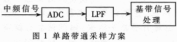
From the point of view of software radio, due to the limitations of the development level of broadband antennas, high-speed A / D converters and digital signal processors, the conditions for achieving an ideal software radio platform [1] are not yet available. Therefore, based on the design requirements of the system with an intermediate frequency of 70MHz and a signal bandwidth of 10MHz, on the basis of analyzing and comparing the advantages and disadvantages of several schemes, this paper focuses on the maximum realization of digitalization of intermediate frequency in the case of existing devices The key issue is to design an intermediate frequency digital receiver that can be used in the experimental platform. In the actual system using this scheme, the key technologies in the new generation cellular mobile communication system can be researched and experimentally evaluated.
1 Preliminary design plan
From the perspective of system flexibility, this article does not consider the intermediate frequency receiving scheme using analog demodulator, but adopts digital processing, and first proposes two schemes.
1.1 A single channel bandpass sampling scheme,
According to the two parameters of the system's intermediate frequency and bandwidth, if low-pass sampling is performed, the Nyquist theorem knows that the sampling rate must be at least 150Msps to ensure that the spectrum does not overlap. However, at the current production level of the chip, ADCs with sampling rates greater than 150Msps and resolutions above 10bit will be very expensive; in addition, the post-level interface circuit must use ultra-high-speed logic circuits, and the pressure of baseband digital signal processing is very large. Increasing the difficulty of wiring and plate-making process of the entire circuit board, which brings many problems. Observe the IF received signal of the system: the highest cut-off frequency is 75MHz, but the signal bandwidth is only 10MHz; if the signal is sampled by low pass, the default signal is distributed in the entire frequency range of 0 ~ 75MHz, this frequency band is no longer used, so the spectrum is The rate is lower. The band-pass sampling mechanism can be used to perform undersampling at a sampling rate much lower than the maximum cut-off frequency of the signal by 2 times, and move the intermediate frequency signal spectrum to baseband without aliasing [1]. The schematic diagram of this scheme is shown in Figure 1. 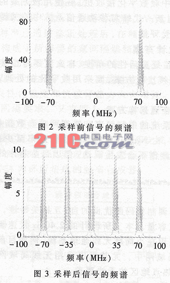
For example, when the baseband signal at the transmitting end is a real signal, select the sampling rate of the receiver fs = 35Msps, and the frequency spectrum is periodically copied to: f1 ± kfs (k is an integer). The changes in the signal spectrum before and after sampling are shown in Figures 2 and 3. Show.
It can be seen from the figure that the band-pass sampling uses the ADC as an approximately ideal mixer to convert the signal. After sampling, the center frequency of the signal is moved from 70MHz to baseband, and the frequency conversion from intermediate frequency to baseband is realized, and the spectrum utilization rate is relatively high. It can be seen that band-pass sampling is a more suitable high-speed IF sampling scheme. The advantage of this scheme is that it no longer requires the ADC to have a high sampling rate, but as long as the sampling rate is selected properly, the back-end can directly obtain the baseband data for corresponding processing, which greatly simplifies the system. The disadvantage of this scheme is that when the transmitted baseband signal is in the form of a complex number, the positive and negative spectra are asymmetric about the imaginary axis. If the sampling rate of 35Msps is still used, the spectrum will be aliased. Therefore, before sampling, the signal is firstly passed through two analog sideband filters to obtain two useful sideband information, and then the bandpass sampling is performed separately. The cutoff characteristic of this analog filter must be very steep, otherwise the passband will be lost Low frequency components within. However, analog filters have two disadvantages: first, filters with a narrow transition bandwidth will cause signal distortion due to the nonlinearity of phase to frequency; second, the narrow transition band means that high-order filters require a large number of high-quality energy storage components, the cost Very high. Therefore, the analog sideband filter is not only expensive, but also distorts the useful signal.
1.2 Two-way orthogonal sampling scheme
The author also proposes a two-way orthogonal sampling scheme suitable for the complex baseband signal at the sending end: borrowing from the basic idea of ​​orthogonal sampling, using two ADCs with the same sampling time at 1/4 intermediate frequency signal period from the initial sampling time Bandpass sampling the IF signal at a rate. Because the phase is 2π as the period, the phase difference of the two sampling signals obtained by this method is π / 2, and they can be regarded as the I and Q of a complex signal respectively. The idea of ​​the scheme is to move the spectrum to baseband. The schematic diagram of this scheme is shown in Figure 4, where NCO (Numberically Controlled Oscillator) represents a numerically controlled oscillator.
This scheme uses two orthogonal signals to recover the baseband complex signal. If you still use the original 1/2 sampling rate, you can get a better signal-to-noise ratio than the first scheme, and the second scheme applies to a wider range. The biggest disadvantage of this scheme is that it requires two ADCs, the complexity of the system grows exponentially, and the starting time of the sampling of the two ADCs must meet about 3.57x10⁻⁹ seconds, and the phase difference between them should be maintained during the sampling process. Unchanged, this requires high phase consistency of the sampling clock and the parameter consistency of the two ADCs, which is difficult for general systems to achieve.
Based on the analysis of its advantages and disadvantages, based on the analysis of its advantages and disadvantages, it weighs the pros and cons in the specific design, and considers the system complexity and system performance trade-offs, forming the following digital reception scheme.
2 Digital receiving solution
2.1 System structure
Based on the above analysis, the author has designed a fully digital receiver based on software radio. The system implementation framework is shown in Figure 5.
This design is based on the first two options, 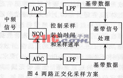 Combined with their respective advantages, they have suppressed their shortcomings as much as possible: on the one hand, due to the application of the band-pass sampling mechanism, this scheme has the advantages of high efficiency and fewer devices used in the first scheme, and it has a wider application range than the first scheme. It can recover the baseband signal in complex form, and the real signal situation realized by the single-channel bandpass sampling scheme is only one special case. On the other hand, the use of a digital downconverter solves the problem of system performance drastically degraded due to inconsistent ADCs circuit parameters and dual-channel amplitude and phase mismatches encountered in the second solution using two ADCs. Therefore, this solution has certain engineering application value, which will be further explained later.
The working process of the system is as follows: the received intermediate frequency signal is passed through a surface acoustic wave SAW (Surface AcousTIc Wave) bandpass filter with a center frequency of 70 MHz: the signal r (t) is obtained after the BPF (Bandpass filter), which is input to the ADC for bandpass sampling , The sampling rate is fs, the generated digital signal r [n] is sent to the digital down converter DDC (Digital Down Converter) for processing, and I and Q baseband data is output to the back-end DSP, FPGA and other digital signals r [n] for processing In the device, different software modules are called to process the specific signals accordingly. This software-based mechanism makes the entire system functions have expandable space, and flexibility is greatly improved.
According to the relevant design index of this system, the band-pass filter adopts BP60190 of VANLONG company. The center frequency is 70MHz, the 3dB bandwidth is 10.2MHz, and the typical insertion loss at the center frequency is 24.7dB. The ADC uses AD9214 from AD Company, which is a 10-bit ADC chip with a maximum sampling rate of 105Msps. DDC adopts AD6624A, a new-generation digital down-converter from AD Company. It represents the highest technical level of multi-channel DDC. One outstanding advantage is that the highest input data rate can reach 100Msps. With this chip, the broadband signals to be received by the system can be sampled at a higher rate, minimizing the deterioration of the signal-to-noise ratio caused by the decrease in sampling rate.
The main functions of AD6624A in this system are down-conversion, low-pass filtering and reducing the sampling rate. The workflow is shown in Figure 5. The real signal r [n] sampled by an ADC is first down-converted by a frequency converter to obtain I and Q. Two signals r1I [n], r1Q [n], so as to avoid the shortcomings of scheme two: Because the quadrature signal in scheme two is sampled by two ADCs, it is difficult to overcome the signal amplitude and phase due to the inconsistency of device parameters Problems such as mismatch. The next stage is a programmable resampling comb filter rCIC2 (second order Resampling Cascaded Integrator
Comb FIR filters). CIC filter is a simple integer coefficient filter, generally considering the signal distortion degree and calculation amount, such filters are often used in engineering to complete extraction or interpolation filtering. The signal then passes through a five-stage cascade comb filter bank CIC5 (frithorder Cascaded Integrator CombFIR filters). Anti-aliasing filtering is performed in the filter bank to obtain baseband signals rI [n] and rQ [n], and data extraction is performed. The extraction rate can be any integer between 2 and 32. Next is the last signal processing unit in AD6624A-programmable RAM coefficient filter RCF (RAM Coeffi-cient FIR filter), in this unit to further transform the sampling rate and shape the signal waveform. Finally, through the output control logic unit, it outputs a low-rate baseband signal that meets the system requirements.
2.2 Determination of main working parameters
Set the working frequency of the internal NCO of the digital down converter (DDC) to fL. Considering the general situation, the baseband signal to be sent is in the form of a complex number, expressed as:
s (t) = I (t) + jQ (t) (1)
Then the intermediate frequency complex signal obtained by up-conversion at the sending end is s1 (t) = s (t) ejωIt, which is modulated by the real part and sent to the radio frequency. Ideally, the IF signal received by the receiver r (t) = Re {s1 (t)}. Among them, Re {·) means taking the real part of the complex number.
The sampled signal r [n] becomes I and Q two signals r1I [n] and r1Q [n] after passing through the frequency converter. Here, only the expression of the I signal is given, and the analysis method of the Q signal is similar . 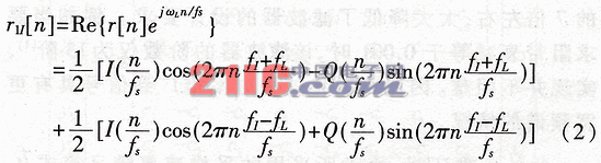
First, we must determine the local oscillator frequency of the NCO in the digital downconverter. Normally, the down-converted local oscillator frequency fL takes a value equal to the intermediate frequency fI, then the second term in equation (2) is the baseband data. But for this system, the intermediate frequency of 70MHz is not within the frequency range that the AD6624A can achieve. Observe formula (2), if fL = fS-fI = 23.3MHz (within the normal operating range of the chip), the second term in the formula is the high-frequency component, which can be filtered by a low-pass filter, so the second The term is a high-frequency component, which can be filtered by a low-pass filter, so the baseband signal r1 [n] = 1 / 2I (n / fs) is obtained. At this time, as long as it is fed into the D / A converter, the I ( t), Q (t) can be obtained in the same way. So this choice of LO frequency can be achieved.
Then determine the optimal sampling rate of the system. The sampling rate of the ADC, that is, the rate of DDG input data, is an important parameter of the entire system. It is restricted by the technical level of the device, and determines the design and selection of the DDC internal filter, decimation rate, and output data rate, which affects the performance of the entire system.
Bandpass sampling theorem requires that the sampling rate meet the following formula to achieve non-aliasing sampling [2]:
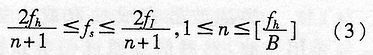
[.] In formula (3) means that the value is not greater than the integer in parentheses. Where fs is the sampling rate, fh and fl are the upper and lower frequency limits of the signal, fh-fl≤fl.
In this system, fh = 75MHz, fl = 65MHz, which can be obtained from formula (3):
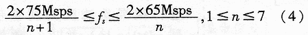
In the sampling rate set given by equation (4), when n = 1, 75Msps≤fs≤130Msps; when n = 2, 50Msps≤fs≤65Msps. An optimal sampling rate is selected to maximize the spectral spacing after sampling, thereby reducing the requirement of anti-aliasing filter out-of-band rejection.
On the other hand, for ADC, if only quantization noise is considered, the expression to measure the ADC signal-to-noise ratio is:
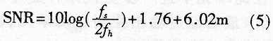
Among them, m is ADC resolution. It can be seen that increasing the sampling rate and A / D resolution can increase the signal-to-noise ratio of the digital signal while keeping people constant. However, the signal itself has a certain signal-to-noise ratio, and it is meaningless for the quantization unit of A / D sampling to be lower than that of noise electrons. Therefore, there is a limit to improving the resolution of A / D. And doubling fs will bring 3dB SNR gain, which is equivalent to increasing the resolution of 0.5bit. You need to take advantage of this in your design and use an optimal sampling rate to achieve better signal-to-noise ratio performance.
Combining the above factors, taking n = 1, the optimal sampling rate is set at 93.333Msps, then the signal-to-noise ratio of the lObit ADC is about 59dB, the spectral spacing of the signal after bandpass sampling is 36.666MHz, and the NCO operating frequency 23.333MHz, the width of the transition band of the anti-aliasing low-pass filter LPF (Lowpass Fiker) can reach 36.666MHz, 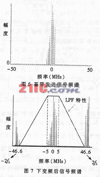 It is about 7 times the single-side bandwidth of the signal, which greatly reduces the filter design requirements. For example, when the stopband attenuation is required to be equal to 0.001, the order of the filter is only 13th order [1], and it is not difficult to achieve. Therefore, this solution can be generalized to the case where the signal has a wider frequency spectrum.
In addition, it is not difficult to prove that because the sampling rate used satisfies the equation fs / 2 = 2fL, the frequency spectrum of the high-frequency component to be filtered after the signal is down-converted is symmetrical, so that the stopband of the low-pass filter can be fully utilized . The following takes s (t) as a multi-tone complex signal with a bandwidth of 10 MHz as an example to illustrate this problem.
Fig. 6 is the spectrum of the transmitted baseband complex signal s (t). Figure 7 shows the frequency spectrum of the signal r1I [n] + ir1 [n] obtained after down conversion of the intermediate frequency receiver. It can be seen that when the fs value is appropriate, the low-pass filter is centered at fs / 2, and is designed to be a stop band symmetrically with 5MHz bandwidths left and right, so that the high frequency components can be filtered out by the stop band. Otherwise, the center of the high-frequency component will be at 40MHz, deviating from 5MHz relative to fs / 2, for example, sampling at 90MHz. When designing a real coefficient FIR low-pass filter, the stop band will be from 35MHz to 55MHz, not only the transition band is narrowed And, only half of the stopband width is used, wasting spectrum resources.
This article is limited to space, and the simulation performance of the above three designs is not mentioned here. Relevant simulation results and analysis and system optimization will be explained in another article.
According to the design goal of establishing a hardware experimental platform for the research of the next three generations of mobile communication systems, this paper proposes a practical engineering design scheme of intermediate frequency digital receiver. Based on the analysis of the signal characteristics of the system, two intermediate frequency receiving schemes based on the band-pass sampling theorem were first proposed, and their respective advantages and disadvantages were pointed out. Then, starting from the requirements of software radio technology for the chip, the first two The advantages of the scheme finally design an intermediate frequency receiver that performs band-pass sampling and uses a digital down-converter, and at the same time determines the key parameters of the actual selected device. Compared with the other two designs in this article, this solution has the advantages of wider application and lower difficulty in implementation.
Dongguan V1 Environmental Technology Co., Ltd. , https://www.v1airpurifier.com