
FPGA vs. ASIC
The development process of the dedicated chip ASIC is: design, verification, tape-out, packaging, and testing;
The FPGA is already a good chip, so there is no need for tape, packaging, and testing. In this way, you can save at least four months.
In addition, the ASIC may be taped multiple times to be successful. Simultaneous software development also requires the chip to complete most functions, which is also a time cost.
When the quantity is small, the cost of FPGA is low, and after the quantity is large, the cost of ASIC is low.
FPGA power consumption is higher than ASIC, because there are a lot of redundant logic, but it saves power than CPU, after all, CPU has more redundant logic.
Compared with ASIC, FPGA debugging is more convenient, you can directly burn to FPGA to execute, you can also use the debugging tool to grab the signal inside the chip to view the status.
How fast does the FPGA need to run?
Compared with the Intel CPU, the main frequency difference of the FPGA is an order of magnitude. Generally, the clock frequency of the FPGA chip is about 300MHz, and the Intel CPU can reach 3GHz, which means that the CPU can do 3 billion calculations per second, while the FPGA can only do 300 million times. 10 times worse.
In addition, FPGA is used as reconfigurable computing to speed up the CPU. It is boring if it runs as fast as the CPU, so it is generally 5 times faster than the CPU.
The development cycle of FPGA is relatively long, one year or even two years is normal. During this process, the software algorithm on the CPU is still continuously upgraded, so it is possible that the FPGA algorithm is designed faster than the CPU. The software algorithms on iterate rapidly and have surpassed FPGA algorithms. This kind of thing is quite common, not only the software algorithm upgrade, but the CPU itself will also be upgraded, which may make the FPGA accelerator useless. For example, using FPGA as a data compression card, but the CPU may bring a data compression function by itself, the cost is still lower than the FPGA card, and the people who develop the FPGA do nothing. Dumb had encountered this kind of problem before. I made an AI algorithm in FPGA. The architecture design was a bit more aggressive. Everyone worked a little slower. After two years of completion, I went to communicate with the person who made AI and found that This algorithm is already an old framework. . .
Therefore, normally, FPGA algorithm acceleration performance design is 5-10 times faster than CPU to ensure that the final product can achieve the goal of hardware acceleration.
Several factors affecting FPGA computing performance
Data parallelism
For FPGA computing, it is best to process a large amount of data at the same time without interdependence. In this way, hundreds or thousands of parallel computing units can independently process hundreds or thousands of data. If there are dependencies between the data, for example, if there are many if else, they cannot be concurrent. A must wait for B to complete before executing. Just go with the Mixed Cavalry of Infantry. If the general orders everyone to march at the same time, the infantry should rush with the cavalry. The cavalry cannot run too fast. They have to wait for the infantry to walk together. Then the battle cannot be fought, and the enemy can only make dumplings. .
2. Data size and computational complexity
FPGA parallel computing is the execution of many calculations in parallel. If each calculation unit has too much data to process and the calculation logic is too complicated, the FPGA computing resources occupied will increase, so that the total number of parallel units will be reduced accordingly and performance will be reduced. . Moreover, the old driver knows that the calculation logic is too complicated, and the more time spent on the circuit will also cause the delay of each module to become longer, so that the clock frequency will also decrease, which will also affect performance.
3. Pipeline
When the calculation is complicated, the delay will become longer. If the calculation task is required to be completed in one clock cycle, the clock cycle will become longer, the corresponding frequency will decrease, and the performance will decrease. Therefore, in order to increase the clock frequency, FPGA will use pipeline technology to decompose complex calculations into several segments and complete them in a few clock cycles. The consequence of this is that the calculation takes longer, but the overall performance is improved. why? Dumb to illustrate.
Eggs originally made 1 toy in 1 hour and 8 in 8 hours a day. Later, the toys were made into eggs, small eggs, and egg mothers. The task was broken down into three sections. Each person took half an hour to make the toys for one and a half hours. However, the total working time of three people per day is 3 * 8 = 24 hours, and 24 / 1.5 = 16 toys are produced per day, and the output has doubled.
This is called three stooges, and one Zhuge Liang has played.


4. Static control logic
When we write software programs, we are used to giving a lot of parameters to the function as conditions, and perform the operation of the function according to the content of the parameters. FPGA does not want to rely on the content of parameters to determine how to calculate, but hopes to set it from the beginning. For example, in the software, calculating the square of single digits is the same as the square of double digits, but in FPGA, single digits require less computing resources and occupy more double digits. A computing unit must support single digits and Two-digit square calculation will be very resource-intensive, it is best to determine which one is good at the beginning, and do not determine it dynamically.
The relationship between storage and calculation
1. Data-intensive and computation-intensive
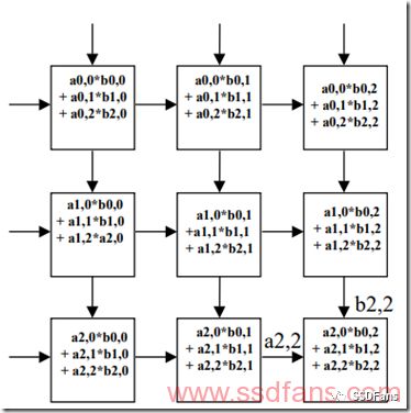
Our calculations are both data-intensive and computationally intensive. If the number of calculations is large, it is computationally intensive, otherwise, it is IO intensive. For example, n × n matrix multiplication, each data read and write is considered to be an IO, reading the data of two matrices and writing the data of the result matrix requires 3n2 IOs, and the number of calculations is n3, so it is computationally intensive . But n × n matrix addition also requires 3n2 IOs, but the number of calculations is only n2, which is IO-intensive.
2. Pulsating array structure
The calculation of AI often involves matrix multiplication and vector multiplication, so storage on the IO side often becomes a performance bottleneck. We often see that in order to solve the "storage wall" problem, the AI ​​chip (such as Google TPU) will use pulsation Array structure, try to achieve data reuse of IO, and convert IO-intensive to computation-intensive. As shown in the figure below, there is data coming in on the left and above, just like a heartbeat, there is continuous blood flow in, but there is a computing array inside, which will not waste the data generated in the middle, all the computing units are working in parallel, resulting in terrible calculations performance.
3. The "storage wall" problem of AI computing
AI calculation requires reading a lot of data. If you rely on the external memory of the AI ​​chip, such as DDR DRAM, latency and performance will be affected. DDR occupies many pins and has high energy consumption. You can only connect one or two, up to 4, There is no way to meet the IO requirements of many parallel computing units. Therefore, it is necessary to place a large amount of SRAM and registers in the chip as on-chip cache in advance, through a lot of small-capacity on-chip RAM, to achieve a large number of concurrent IO, to provide hundreds of parallel computing engines.


To solve the storage wall problem, there are two paths:
(1) 3D stacking based on HBM (High-bandwidth Memory) technology, many memory chips and AI chips are packaged together. Both AMD and NVIDIA's Vega and Volta GPUs integrate 16GB of HBM2. Some of the latest AI chip architectures of other companies also integrate 3D stacked storage. For example, Intel Nervana also uses 3D HBM, while Wave Computing uses Micron ’s HMC, another form of 3D stacked storage. Google's TPU 2.0 also uses 8GB of HBM per core.
(2) Integration of computing and storage. The storage medium and the AI ​​calculation engine integrated with a new type of RRAM and other data that do not lose data are integrated into a single chip. The data has always been stored in the AI ​​chip and does not need to be loaded from the outside, reducing data movement, and the efficiency and performance are very high. For example, the team of Professor Xie Yuan of the University of California put neural network computing and RRAM in a chip, which can reduce power consumption by 20 times and increase speed by 50 times. IBM also published an article in Nature, announcing that the same neural network computing for AI applications has been implemented on phase-change memory.

We use FPGA for computing. There is a very important concept called Domain Specific Computing, which was proposed by Professor Cong Jingsheng of UCLA. It is a special optimization of hardware algorithms for computing tasks in a certain field, mainly performance improvement and algorithms. Compression to achieve high performance and low cost.
FPGA to do the first calculation of axe: turning motion into static
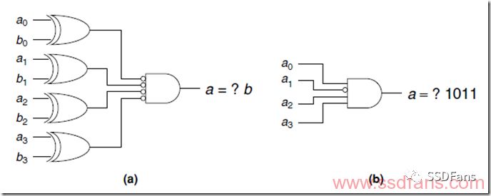
As mentioned before, if FPGA performs different computing tasks according to a certain parameter, it is a waste of resources, because each kind of computing engine must be implemented with hardware computing resources, waiting for users to use. If we know that the computing tasks are fixed for a period of time, we can configure the FPGA to have only one computing task, saving resources and enhancing computing power.
The other case is called constant folding. If we find that a variable will not change for a period of time, we can use it as a constant without occupying the calculation logic. As shown in the figure below, it was originally two 4-bit number a and b comparators, but it is known that b is 1011, you can directly use a to output the result, saving 4 logic gates.
FPGA to do the second calculation: real-time reconfiguration
The current FPGA supports real-time reconfiguration of the computing logic inside, and the entire FPGA can be reconfigured into new logic, for example, the last millisecond is aPU and the next millisecond is bPU. More practical is the real-time reconfiguration of part of the logic, because many of the logic in the FPGA is used for control and does not need to be changed frequently, but the part of the calculation should be changed frequently according to the usage, so real-time reconfiguration of a certain partition is supported.
FPGA to do the third calculation: bit width compression
We write software programs and are accustomed to the addition, subtraction, multiplication and division of two 32-bit or 64-bit variables, because everyone shares a CPU calculation unit and does not waste resources. But in the FPGA, it is a kind of parallel computing. Every program occupies computing resources, so it can be saved. For example, if two 32-bit numbers are multiplied, if we already know that there are only two bits of valid data for a certain number, we only need to represent it with 2 bits, and then the final result can be shifted.
In the final analysis, as long as we understand that the two advantages of fast FPGA computing are parallel and pipeline, but we must always have the idea of ​​parallel computing, try to compress the resources occupied by the algorithm, so as to achieve the most powerful parallel computing power with limited FPGA computing resources.
LCD drivers use FrameBuffer technology, so LCD drivers are also known as FrameBuffer drivers.
Liquid Crystal Display Monitor is a Liquid Crystal Display with a monitoring BNC signal processing terminal using a 7*24 hours professional power module and a monitoring driver scheme using Liquid Crystal Display technology.
contrast
Contrast, as opposed to brightness, is the main measure of an LCD monitor. Generally, the contrast ratio of Shanghai shadow display reaches 350:1, which can satisfy the function of normal display of computer, TV and other images; For the monitor LCD monitor, because the product itself has high requirements for the image, the general LCD monitor will sacrifice color parameters to improve the contrast and brightness of the whole machine.
So in general, use LCD monitor to see TV color effect is not as good as LCD TV, but LCD monitor contrast, clarity, brightness will be much higher than LCD, LCD TV.
resolution
Resolution refers to the number of horizontal and vertical liquid crystal lines on the LCD screen. Resolution is the most important index to evaluate a LCD monitor. We are talking about the physical resolution of the LCD monitor, not the maximum resolution that can be achieved.
LCD driver
Liquid crystal drive program, namely liquid crystal display drive board actually. Select different driver board, there will be different display effect. What general TELEVISION USES is TV 3 in 1 board. Support VGA, S terminal, AV signal. This kind of board mainly pays attention to the overall display color and saturation, resolution generally adopts standard 1366*768. So the LCD monitor modified by TV is relatively good when connected with TV signal.
Open Frame Lcd,Open Frame Touch Screen,Open Frame Lcd Monitor,Open Frame Touch Screen Monitor
TONYA DISPLAY LIMITED , https://www.tydisplay.com