During the LED packaging process, electrode contamination often occurs after solid crystal baking. This paper investigates the nature of these contaminants and identifies them as volatile components from solid oxide gels. Based on this analysis, two potential causes for electrode adhesion are explored, along with practical solutions to address the issue.
One: Electrode Contamination
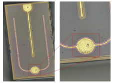
In current LED packaging processes, after the solid crystal glue is baked and cured, contaminants can adhere to the gold electrodes, leading to issues such as poor wire bonding or insufficient wire pull force. As shown in the image below, a metallographic microscope reveals significant contamination on the electrode surface.
Two: Cause Analysis and Solutions
1. Contaminant Composition
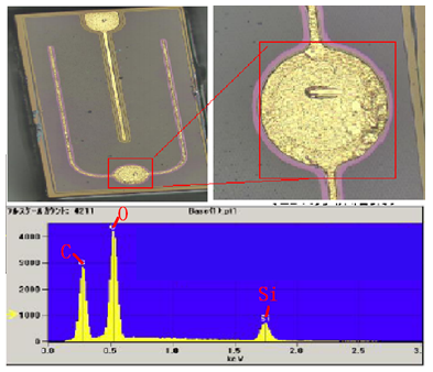
Using an Energy Dispersive Spectrometer (EDS), we analyzed the contaminated areas of the chip and found elements such as carbon (C), oxygen (O), and silicon (Si). These correspond to the main components of the solid crystal glue, which is primarily composed of siloxane. Although EDS cannot detect hydrogen (H), it is reasonable to infer that the contaminant contains components from the solid crystal glue.
2. Cause Analysis
Based on elemental analysis, we suspect that the contaminant is derived from the solid crystal glue. During baking, the glue may interact with the electrode surface. However, no signs of creeping were observed around the chip, suggesting that direct contamination from the glue is unlikely. Instead, during the curing process, small amounts of volatile compounds, including hydroxyl-containing cross-linkers, may be released. These compounds have high chemical activity and could contribute to electrode contamination.
2.1 Hydroxyl-Containing Small Molecule Cross-Linker and Chemical Adsorption
2.1.1 Source of Chip Contaminants
Contamination may come from the manufacturing process or from handling during die bonding. Microscopic inspection showed no visible signs of fingerprints or other external contaminants, indicating that manual operations are not the primary source. However, during photolithography, developers like sodium carbonate solution may leave residual hydroxyl groups on the electrode surface. If cleaning steps are incomplete, these residues could react with the cross-linking agents in the solid crystal glue.

2.1.2 Source of Solid Crystal Glue Volatiles
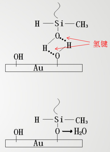
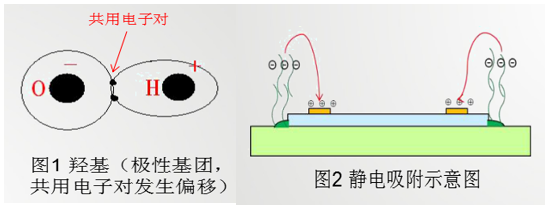
The hydroxyl-containing cross-linkers in the solid crystal glue have short molecular chains and low boiling points, making them prone to volatilization during heating. These molecules can form hydrogen bonds with hydroxyl groups on the electrode surface, leading to adsorption and eventual contamination.
What is a hydrogen bond?
A hydrogen bond occurs when a hydrogen atom bonded to a highly electronegative atom (like O, F, or N) interacts with another electronegative atom. This interaction, represented as XH...Y, plays a key role in many chemical and biological processes.

2.1.3 Reaction Process
As shown in the diagram, hydroxyl groups from the cross-linker can form hydrogen bonds with hydroxyl groups on the electrode. Some of these bonds may convert into covalent bonds, releasing water molecules in the process. Over time, more cross-linkers react, leaving behind solid crystal glue residues containing C, O, and Si.
2.1.4 Experimental Verification
Chips were divided into two groups. One was soaked in an alkaline solution, while the other remained untreated. After applying solid crystal glue and baking, the treated group showed significant contamination, confirming that hydroxyl groups on the electrode reacted with the glue's volatile components.

2.1.5 Solution
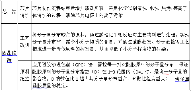
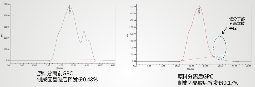
To reduce contamination, both the chip and the solid crystal glue must be improved. By removing small molecular substances through distillation, the volatile content of the glue was reduced from 0.48% to 0.17%, significantly decreasing electrode pollution.
2.2 Hydroxyl-Containing Small Molecule Cross-Linker and Electrostatic Adsorption
2.2.1 Causes of Chip Charging
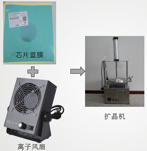
During chip expansion, static electricity can be generated when peeling off the blue film. Proper procedures require the use of ion fans and wristbands to prevent static buildup. However, some operators neglect these steps, increasing the risk of electrostatic contamination.
2.2.2 Electrostatic Adsorption Mechanism
The hydroxyl group in the cross-linker is polar, and if the electrode is charged, it can attract these molecules via electrostatic forces. This leads to accumulation and contamination on the electrode surface, affecting wire bonding.
2.2.3 Experimental Verification
Chips were tested under different conditions—some were charged, others were neutralized. The results showed that charged chips had much more contamination, confirming the role of electrostatic attraction in the process.

2.2.4 Solution
To address electrostatic-related contamination, both operational procedures and glue formulations must be improved. Ensuring proper static control and using cleaner glues can significantly reduce electrode contamination.

Three: Summary
After thorough analysis, it was determined that the contaminant is primarily solid crystal glue. Two mechanisms were identified: chemical adsorption due to hydroxyl groups and electrostatic attraction. Experiments confirmed that chemical adsorption is the main cause, while electrostatic effects are secondary. To resolve this, improvements in both the chip preparation and glue formulation are essential.

References:
Liu Xing. Mechanism of silane molecule adsorption and film formation kinetics on metal surface [D]. China University of Geosciences (Wuhan), 2012.
Geng Yiping, Tang Bing, Huang Shuhuan. Advances in Adsorption of Organic Substances on Metal Surfaces[J].Surface Technology, 2009, 38(2):70-72.
Author: Fang Huayu, Pei Xiaoming

USB 2.0 standard offers data transfer speeds of up to 480 Mbps, making it suitable for most common peripherals and devices.This hub is backward compatible with USB 1.1 devices, ensuring that you can connect older devices without any issues.
It often comes with a separate power adapter to provide sufficient power to all the connected devices, ensuring stable and reliable performance.
16-Port USB 2.0 Hubs may include additional features like LED indicators for each port, allowing you to easily identify which ports are in use.This can be particularly useful when dealing with a large number of connected devices.
Hubs offer overcurrent protection, which safeguards your devices from potential damage caused by power surges or short circuits.This feature ensures the safety of your valuable equipment.
16-Port USB 2.0 Hub is an excellent solution for individuals or businesses that require multiple USB connections.It provides convenience, flexibility, and efficiency by expanding the connectivity options of your computer or laptop, allowing you to connect and use multiple devices simultaneously. Whether you are a professional or a tech enthusiast, this hub can greatly enhance your productivity and simplify your daily tasks.
Multi-port intelligent A-port hub,16-Ports HUB2.0,16-port A-port cabinet type hub,Smart USB2.0 hub
shenzhen ns-idae technology co.,ltd , https://www.best-charger.com
