
The LTC4366 surge suppressor protects the load from high voltage transients. By controlling the gate of an external N-channel MOSFET, the LTC4366 regulates the output during overvoltage transients. With overvoltage across the MOSFET, the load can remain operational. Deploying a resistor in the return line isolates the LTC4366 and allows it to float up with the power supply; therefore, the upper limit of the output voltage depends only on the availability of the high value resistor and the MOSFET's rated specifications.
An adjustable overvoltage timer prevents damage to the MOSFET during a surge, while an additional 9s timer provides a cooling cycle for the MOSFET. The shutdown pin is responsible for reducing the quiescent current to less than 14A during shutdown. After a fault occurs, the LTC4366-1 will be locked and the LTC4366-2 will perform an automatic retry operation.

Application information
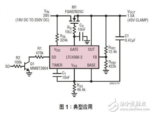
A typical application of the LTC4366 is a system that requires overvoltage protection that safely distributes power to the load during overvoltage transients. The selection of external components is discussed below.
Double shunt regulator
The LTC4366 uses two shunt regulators with external buck resistors, RSS and RIN, to create internal supply rails on the VDD and OUT pins. These shunt regulated power rails provide overvoltage protection for high voltage transients with unlimited input voltage to the circuit, regardless of the RTX4366's internal circuit voltage rating.
At the start of the start, during the shutdown, or after an overvoltage fault, the GATE pin voltage is clamped to the OUT pin, thereby turning off the MOSFET. This allows the VSS and OUT pins to be pulled to ground using the output load and RSS. In this case, the VDD pin voltage is clamped to VSS with a 12V shunt regulator. Then, (complete power supply voltage – 12V) is applied to the RIN resistor responsible for setting the shunt current. The shunt current can be as high as 10 mA, which is orders of magnitude higher than the typical quiescent current of VDD 9A.
In normal operating mode, the OUT voltage is equal to the input supply voltage. When C1 is fully charged, IC1 is zero at this point. In this case, the voltage between the OUT and VSS pins is clamped using a 5.7V shunt regulator. (Input supply voltage – 5.7V) is added to the RSS. The RSS current is divided into three blocks: a 5.7V shunt current, a bias current between OUT and VSS, and a final RIN current. The 5.7V shunt current can be as high as 10mA, which greatly exceeds the typical OUT (160A) bias current.
Boot timing
After the input supply rises, the voltage between the VDD and VSS pins is adjusted in parallel to 12V. Next, the internally generated power supply VCC generates a 30 s power-on reset pulse that will clear the fault latch and initialize the internal latch. The shutdown comparator then determines if the SD pin is pulled low externally, and if YES, requests a low bias current shutdown condition. Otherwise the external MOSFET M1 will be allowed to turn on.
Accessing from the VDD pin, powering up the MOSFET gate through a 7.5AGATE pull-up current source is known as the "bootstrap" method. When the GATE voltage reaches the VDD pin voltage (minus a Schottky diode voltage drop), the 7.5A current source loses its voltage drop and stops charging GATE (the waveform in the middle of Figure 2). The bootstrap method relies on charging C1 to a sufficient voltage after the GATE pin voltage has stopped rising. The voltage on C1 is then used as a power source for a charge pump that charges the gate to its final value (ie, OUT + 12V). If the charge pump current exceeds the C1 charge current, C1 will discharge. If the C1 voltage is below 4.35V, the charge pump will suspend operation and recharge C1.
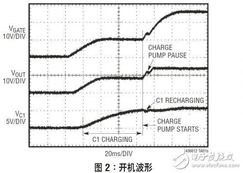
If the power is turned on and the C1 cannot be charged under heavy load conditions, it may cause overheating and damage to the device. When the gate and output ramps up, the voltage drop across the MOSFET is the input supply voltage minus the output voltage. If the supply voltage is lower than the value required for C1 charging, the output will not ramp up beyond (supply voltage – MOSFET threshold). This 3V to 5V MOSFET voltage drop and high load current will result in power dissipation without any protection or timeout limits.
Overvoltage fault
The LTC4366 prevents overvoltage on the input supply from reaching the load. Typically, the pass transistor is fully turned on and supplies power to the load with a very small voltage drop. As the input voltage increases, the OUT voltage increases until it reaches the regulation point (VREG). From this point on, any further voltage increase will fall across the MOSFET. Note that since the MOSFET is still on, the LTC4366 provides uninterrupted operation during short overvoltages.
The VREG regulation point is configured with two FB resistors (RFB1 and RFB2). The regulation amplifier is responsible for comparing the FB pin voltage to (threshold OUT pin voltage – 1.23V). The voltage drop across RFB1 during regulation is 1.23V, while the remaining VREG voltage drops across RFB2. When the output is at the regulation point, a timer is started to avoid excessive power dissipation in the MOSFET. The TIMER pin is typically held low using a 1.8A pull-down current. During regulation, the TIMER pin is charged with a current of 9A. If the regulation point is held long enough for the TIMER pin voltage to reach 2.8V, an overvoltage fault lock is generated. The formula used to set the timer capacitor is:
CT=3.5?t[nF/ms]
Depending on the version, the device will cool down and start automatically (LTC4366-2), or remain latched until the SD pin initiates a restart (LTC4366-1). The cooling time is typically 9 seconds, which provides a very low pulse power supply duty cycle.
Starting at input supply overvoltage and full load current does cause the MOSFET's power dissipation far beyond the level of a typical overvoltage surge. During the ramping of the gate and output voltage, some of the supply voltage (at full current) drops across the MOSFET. After startup, a normal overvoltage surge occurs before the MOSFET turns off. For safe working area (SOA) calculations of MOSFETs, the “Design Examples†section only considers normal overvoltage surges. Starting in an overvoltage situation will require more consideration for SOA.
Downtime
The LTC4366 has a low current ("20A" shutdown state that can be used to turn off the transfer FET by using a switching resistor to connect the GATE and OUT pins together. Under normal operating conditions, a 1.6A current source pulls the SD pin up to the VDD pin voltage. When the shutdown state is not used, the SD pin is connected to VDD. Pulling the SD pin below (VDD pin voltage –1.5V) for more than 700s of filter time will initiate a shutdown condition. This filter time is used to avoid undesired shutdown starts during transients. The SD pin is clamped to VSS–0.7V by a diode, which requires a current limit on the pull-down device (maximum 10mA). One of the methods of current limiting is to connect an external 470k resistor in series with the open collector pull-down device. Starting the external pull-down current source will exceed the internal 1.6A pull-up current source and cause the SD pin voltage to cross the shutdown threshold. After an overvoltage fault, placing the device in a shutdown state will clear the fault and resume operation as soon as the LTC4366 exits the shutdown state.
Commercial Blenders are our new product series. We have a full range of commercial blenders, including rotary switch commercial blenders, push button commercial blenders, LED touch panel commercial blenders, etc. All of our commercial blenders jar are PC unbreakable jar, very strong and sturdy.
Discription of Commercial Blenders
Size: 2L, 3L
Jar Material: PC unbreakable jar
Controls Type: Rotary switch, push button, LED touch panel

Commercial Blenders
Commercial Blenders,Commercial Blender Vitamix,Large Commercial Blender,Waring Commercial Immersion Blender
Flying Electronic Co., Ltd , https://www.flyingelectronic.com