
Recent advances in ADC design have greatly expanded the available input range so that system designers can remove at least one intermediate frequency stage, thereby reducing cost and power consumption. Special attention must be paid to sampling clocks in undersampling receiver designs because clock jitter can be a major cause of limiting signal-to-noise ratio (SNR) at high input frequencies. This article focuses on how to accurately estimate the jitter of a clock source and how it can be combined with the aperture jitter of the ADC.
Review of the sampling process
According to the Nyquist-Shannon sampling theorem, if the original input signal is sampled at a rate at least twice its maximum frequency, it can be fully reconstructed. Assuming a sample signal of up to 10MHz is sampled at a rate of 100 MSPS, it doesn't matter whether the signal is in the baseband from 1 to 10 MHz (the first Nyquist region) or undersampled in the higher Nyquist region from 100 to 110 MHz (please See Figure 1).
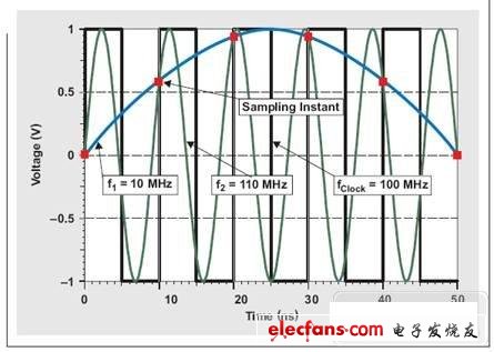
Figure 1 Two input signals sampled by 100MSPS show the same sample points brought by aliasing
Sampling in higher (second, third, etc.) Nyquist regions is generally referred to as undersampling or subsampling. However, anti-aliasing filtering is required in front of the ADC to sample the ideal Nyquist region while avoiding interference during the reconstruction of the original signal.
Time domain jitter
Looking closely at a sample point, you can see how timing changes (clock jitter or clock phase noise) form amplitude changes. Due to the increase in input frequency due to undersampling of high Nyquist regions (eg, f1 = 10 MHz to f2 = 110 MHz), a fixed amount of clock jitter produces a greater amount of amplitude deviation (noise) from the ideal sample point. In addition, Figure 2 shows that the clock signal's own slew rate affects the change in sampling time. The slew rate determines how fast the clock signal passes through the zero crossing. In other words, the slew rate directly affects the trigger threshold of the clock circuit in the ADC.
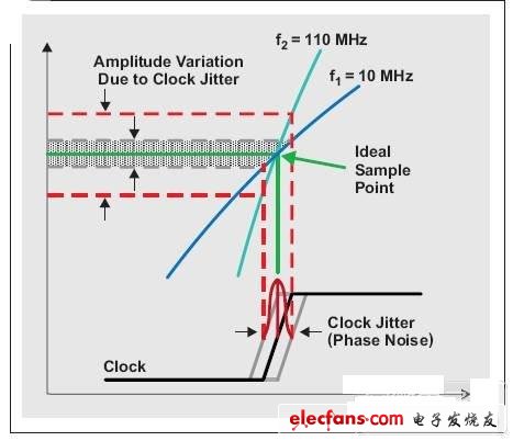
Figure 2 Clock jitter forms more fast input signal amplitude error
If there is a fixed amount of thermal noise on the ADC's internal clock buffer, the slew rate is also converted to a timing error, which reduces the ADC's inherent window jitter. As shown in Figure 3, window jitter is not related to clock jitter (phase noise), but the two jitter components are combined at the sampling time.
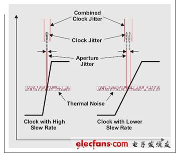
Figure 3 ADC window jitter
Figure 3 also shows that window jitter increases as the slew rate decreases. The slew rate is generally directly dependent on the clock amplitude.
Rectangular I/O Connectors
Antenk offers an expansive product line of I/O Connectors including USB, HDMI, D-Sub, Modular Jacks, SFP, QSFP+, CXP, iPass+, iPass+ HD and more. In addition to standard I/O connectors and matching cable assemblies.Except a comprehensive range of standard Input/Output connector solutions for high-speed electronic data communication, Antenk engineers can design customized solutions. This extensive selection of I/O connectors and matching cable assemblies includes numerous next-generation solutions.All of our I/O connectors feature a variety of orientation options, as well as PCB and cable mount offerings.
Antenk develop and specify high-performance I/O's throughout a wide variety of industries. These include SAS, SATA, PCIe, HSSG, FIBRE CHANNEL, INFINIBAND, IEC, CEA, IEEE, VESA, USB and many more.
I/O Connectors Application
Consumer / PC Products
Networking / Telecommunications Products
Mobile Products
Industrial Products
Antenk can deliver standard and custom options of the following I/O connectors:
1394 Connector
Centronic Connector
D-Sub Connector
DVI Connector
Display Port Connector
HDMI Connector
Half Pitch Scsi Connectors
USB Connector
V.35 Connector
OBD Connector
I/O Connectors General Specifications


ELECTRICAL CHARACTERISTICS
Contact Current Rating:5Amperes.
Dielectric Withstanding.
Dielectric Withstanding Voltage:AC 1000Vr.m.s.
Insulation Resistance:500 Megohms Minimum at DC500V.
Contact Resistance:25 Milliohms Maximum.
Operating Temperature:-55℃~105℃.
")
MATERIALS:
Contacts:Brass.
Insulator:PBT,UL94V-O Rated.
Shell:Cold Rolle Steel.
Metal Watertight Frame:PBT,UL94V-0.
O-Ring:Silicone.
NOTE:
Position:09PIN,15PIN,25PIN,37PIN.
Rectangular I/O Connectors
Rectangular Connector,Rectangular I Connectors,Rectangular O Connectors,Male Connector Rectangular,I/O Connectors,Input/Output Connectors
ShenZhen Antenk Electronics Co,Ltd , https://www.antenk.com