
For more than 50 years, synthetic diamonds made with high-pressure high-temperature technology (HPHT) have been widely used in grinding applications, giving full play to the extremely high hardness and extremely high wear resistance of diamonds. In the past 20 years, new methods of diamond formation based on chemical vapor deposition (CVD) have been put into commercial use, which has resulted in the production of single crystal and polycrystalline diamond at a lower cost. These new synthetic methods support the full development of the optical, thermal, electrochemical, chemical, and electronic properties of diamond.
Diamond has been widely used in the optical and semiconductor industries. This paper mainly discusses the thermal advantages of diamond, introduces the working principle of diamond heat sink, briefly introduces the diamond generation method, summarizes some common applications of diamond (including application methods) and draws conclusions on the future application prospect of diamond. First, let us briefly introduce the reason and principle of diamond becoming the best thermal conductor in all solid materials at room temperature.
Diamond heat conduction principleDiamond is a cubic crystal formed by covalent bonding of carbon atoms. Many of the ultimate properties of diamond are direct results of the strength of the sp3 covalent bond forming a rigid structure and the action of a small amount of carbon atoms.
Metals conduct heat through free electrons, and their high thermal conductivity is associated with high electrical conductivity. In contrast, heat conduction in diamond is only done by lattice vibration (ie, phonons). The strong covalent bond between the diamond atoms makes the rigid lattice have a high vibration frequency, so its Debye characteristic temperature is as high as 2,220 °K. Since most applications are much lower than the Debye temperature and the phonon scattering is small, the phonon-mediated heat transfer resistance is extremely small. However, any lattice defect produces phonon scattering, which reduces thermal conductivity, which is an inherent feature of all crystalline materials. Defects in diamonds typically include heavier l3C isotopes, nitrogen impurities and vacancy defects, stacking faults and dislocations, and other 2D defects such as grain boundaries.
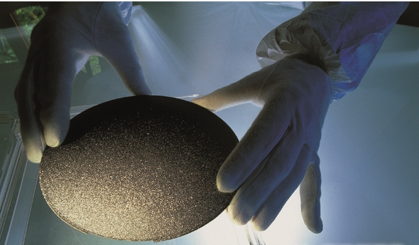
Figure 1. Freestanding CVD Diamond Wafer
As a component specifically designed for thermal management, natural diamond is used in some early microwave and laser diode devices [1], [2]. However, the availability, size and cost of a suitable natural diamond plate limit the market application of diamond. With the advent of microwave-assisted CVD polycrystalline diamond with thermal properties similar to Type IIa natural diamond (Figure 1), usability issues have been resolved. Currently, many suppliers offer a range of ready-made thermal grade diamonds. Since the free-standing polycrystalline diamond is generated from a large wafer (Fig. 1) with a diameter of 140 mm, the size is no longer limited to a single device or a small array, and the array size can be extended to several centimeters. For the above reasons, the practicality of CVD diamond has been verified and has been widely used in various devices since the 1990s.
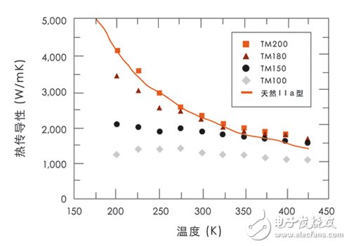
Figure 2. Comparison of thermal conductivity and temperature between layers measured by Type IIa natural diamond laser flash method
As shown in Figure 2, TM200 (TM means heat, 200 means thermal conductivity) 2,000 Wm Ì„lK Ì„l) The thermal conductivity at room temperature is 2,200 Wm Ì„lK Ì„l, which exceeds the thermal conductivity of copper by 5 times ( See Table 1). Element Six offers a range of products, so thermal conductivity and cost can be tailored to your technical requirements and budget. Due to the thermal conductivity "1,000 Wm Ì„l K Ì„l at room temperature, TM100 exceeds 4 to 6 times the ceramic material such as aluminum nitride.
Advanced products have an advantage in thermal performance below room temperature, and thermal conductivity is significantly improved at temperatures as low as 100 °K. The TM180 and TM200 ratings in Figure 2 show similar performance and temperature trends as Type IIa natural diamond.
We used characterization techniques to analyze different levels of microstructure. Within the scope of the study, the conductivity of the TM100 is less sensitive to temperature. The grain size in CVD diamond increases with increasing thickness and has a significant effect on the conductivity. For CVD diamonds of the same grain size, the point defect densities are similar in TM100 and TM180, but the misalignment density in TM100 is three orders of magnitude higher than TM180. This difference plays a major role in phonon scattering and has a significant effect on the conductivity. The misalignment density measured in the TM180 and TM200 is similar, but the small difference in conductivity at lower temperatures can be explained by the grain size and the point defect density in the TM200, which is 5 times lower than the TM180. In the following paragraphs of this paper, we will explore other generation techniques. The grain size, purity, and misalignment of each generation technology are significant, so there are also large differences in thermal performance.
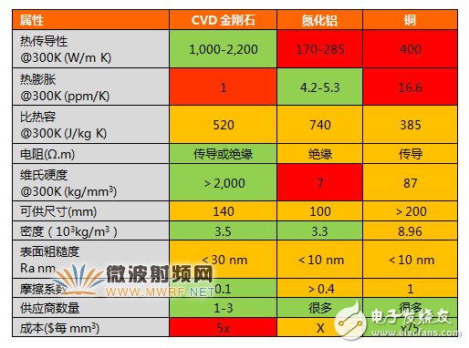
Table 1. Green = significant advantage, yellow = medium advantage, red = negative impact
The power density in the field of power converters or solid-state RF power amplifiers in the semiconductor market continues to increase, making local thermal management burdens heavier. CVD diamond has the ultimate properties of high thermal conductivity and electrical insulation, and is an ideal solution to the above problems. Our measurements show that the ratio of the conductivity between the layers in the microwave-assisted CVD diamond layer is less than 10%, which is comparable to the measurement uncertainty. Isotropic thermal properties and electrical insulation are important attributes of heat sinks in many thermal applications. This is in sharp contrast to materials such as highly oriented pyrolytic graphite, which is electrically conductive and thermally conductive, as shown in Table 2.
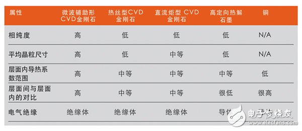
Table 2. Comparison of thermal properties of polycrystalline diamond synthesized by different CVD techniques.
Diamond generation methodSynthetic diamond is manufactured using a range of different technologies. Synthetic diamond particle size, large single crystal and sintered polycrystalline diamond products are synthesized by high pressure and high temperature pressing technology. The highest purity single crystal diamond products are made by microwave assisted CVD, but polycrystalline CVD diamonds can be fabricated using different techniques. As shown in Table 2, there are differences in the properties of diamonds produced by different techniques. In general, diamond CVD can be divided into three categories: microwave assisted CVD, hot filament CVD, and DC arc or DC torch CVD.
In various CVDs, the same point is a small amount of gas phase carbon component in hydrogen gas, and the gas temperature exceeds 2,000 °K to cause H2 to decompose into a highly reactive H&TImes; Hot filament reactors typically have a sedimentation diameter of up to 300 mm, but the balance between sedimentation area, uniformity (such as purity) and yield is critical and is as important as overall performance. Phase purity (affected by the reduction in sp2 content) can be controlled by two methods: (1) reducing the input methane flow rate and rate of formation (but increasing generation time and cost), and (2) increasing the H2 decomposition rate by increasing the gas temperature. Microwave and DC arc spray reactors are more likely to increase gas temperature. Microwave-assisted CVD allows for optimal impurity content control because it eliminates the need for a cathode or filament, maximizing the purity, optical transmission, and thermal conductivity of microwave-assisted CVD diamond.
CVD diamond heat dissipation applicationFactors to consider when integrating CVD diamond in a thermal system
To successfully integrate thermal management components into the device, the complete thermal conduction path as well as electrical requirements and thermo-mechanical stress must be considered. Although CVD diamonds are extremely rigid and have a small coefficient of thermal expansion (approximately 1 ppm/K), they are ideal for high power transmission window applications due to their compatibility with Si (2.6 ppm/K), GaAs (5.7 ppm/K) and There are significant differences in common semiconductor materials such as GaN (3.2 – 5.6 ppm/K), which poses significant challenges for thermal design engineers. Unless considered at the beginning of the design, the stress generated by the thermal cycle can adversely affect device life and reliability. The two methods of controlling these stresses are composite semiconductor pre-cracking [6] and diamond interlayer; in the diamond interlayer, the upper layer is used to balance stress. When integrating diamond into a device package, the ideal geometry depends on many factors such as power density, cooling channel location, etc., but the model design is simple.
Fig. 3. Metallized CVD diamond heat sink
CVD diamond can be widely integrated into thermal solutions in three ways: (i) Separate individual diamond units are bonded by metallization and soldering, see Figure 3 (eg, depositing metal and AuSn eutectic with TI/Pt/Au sputtering) Soldering); (ii) Prefabricated wafers support multiple devices, enabling device manufacturers to process wafers in large quantities (such as metallization and placement). After such additional steps are completed, the wafers can serve as a substrate for a single subassembly. (iii) Direct diamond coating.
Laser diode arrayUsing CVD diamond as the interface between the laser diode array and the microchannel cooling copper block, the device temperature rises from 22 ° C to 16 ° C, as shown in Figure 4, significantly extending product life.
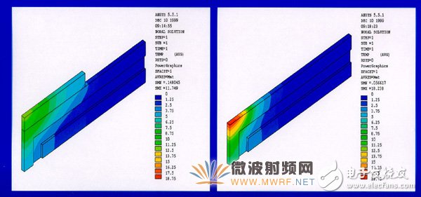
Figure 4. Copper microchannel heat sink model with and without CVD diamond heat sink under the device. The peak temperature rises from 22 ° C (red) to 16 ° C (green).
The laser diode array (peak power density of 100 W/mm2 at 200 μm intervals) changes the CVD diamond geometry on a simple cooled copper block, indicating that a 300 μm thick 3 mm wide diamond is required instead of a thin diamond coating. It should be noted that the experimental results modeling comparison shows that metallization is also an important part of the heat conduction path. Typical metallization is TI/Pt/Au with a total thickness of approximately 1 μm [7]. The titanium layer is a key factor in adhesion and forms a carbonized layer at the interface with the diamond. The gold layer provides a low resistance connection and serves as a base layer for subsequent soldering or wire bonding. The platinum layer serves as a barrier to prevent copper from diffusing to form excess intermetallic compounds.
RF module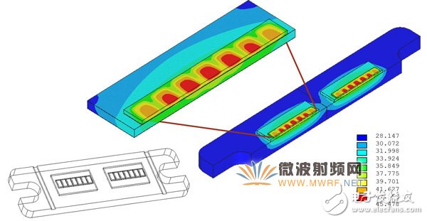
Figure 5. (a) RF package simulation of integrated discrete RF devices on a BeO heat sink bonded to a CuW flange.
Another example is a radio frequency package consisting of discrete RF devices connected to a 1 mm thick yttria heat sink mounted on a CuW flange. Cerium oxide is toxic and its thermal conductivity is only about 200 Wm ~ lK ̄l. The thermal model (Figure 5) shows that replacing the yttrium oxide with 300 μm thick TM100 CVD diamond can reduce the thermal resistance by 30%. The overall package temperature drop measurement collected by the infrared camera shows the maximum temperature drop across the device and the CuW flange, and also shows that the diamond layer temperature drop is negligible. At present, the product has been mass-produced, and the output at the same junction temperature is increased by 40% by means of CVD diamond.
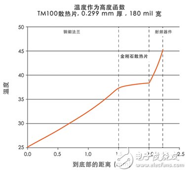
Figure 5. (b) Measurement results for the entire package temperature drop collected using an infrared camera.
Diamond application prospectsThe use of CVD diamond as a heat sink in the semiconductor industry is still in its infancy. Optoelectronic, power and RF devices are increasingly demanding superior thermal management solutions that will drive the widespread adoption of this engineering material over the next decade. Combined with the growth rate of these market segments, the increase in diamond adoption rate will drive large investments into the synthetic diamond manufacturing industry, which will promote economies of scale and make diamonds a place in the semiconductor market that was previously unable to compete.
In the next decade, we can expect semiconductor manufacturers to integrate diamond as a substrate into their devices for commercialization. For example, GaN combined with diamond theoretically provides 120 Wcm Ì„2 of power consumption compared to 40 Wcm Ì„2 for SiC.
At the same time, we also expect CVD diamonds with high thermal conductivity and high breakdown voltage characteristics to be used as active semiconductors. Initially it may be mainly used in the field of high voltage switches, but as the technology matures, other applications will continue to emerge.
Encoding disk refers to a digital encoder that measures angular displacement. It has the advantages of strong resolving power, high measurement accuracy and reliable work. It is one of the most commonly used displacement sensors for measuring the position of the shaft rotation angle. The code disk is divided into two types: absolute encoder and incremental encoder. The former can directly give the digital code corresponding to the angular position; the latter uses a computing system to make the pulse increment generated by the rotating code disc against a certain reference number addition and subtraction. The metal encoding disk is directly engraved with through and unconnected lines, and it is not fragile, but because the metal is not easy to corrode but easy deform, the accuracy is limited, and its thermal stability is an order of magnitude worse than that of glass. It is mainly used in motor, hardware, electrical appliances, automobile and other fields.
We customize diverse patterns metal encoder disk with drawings provided by customers. We are equipped with professional metal etching equipment and exposure development equipment. The raw material use for encoder disk are SUS304 stainless steel and the flat degree can below 0.02 mm. Our stainless-steel encoder disk can achieve flat, no burr and can be available in harsh environment.
Stainless Steel Encoder Disk,Encoder Disk,Metal Encoding Disk
SHAOXING HUALI ELECTRONICS CO., LTD. , https://www.cnsxhuali.com