
Active Electrical Array (AESA) radar is a key component of today's advanced weapon systems, especially airborne combat systems. The future development of its architecture will extend beyond the initial military applications to geophysical mapping, automotive assisted driving, automated vehicles, industrial robots and augmented reality: in fact, this includes any need to condition large amounts of sensor data. An application that incorporates into the model for decision making.
As the AESA architecture expands, they will break through radar signal processing professional applications and extend to other applications. In external applications, these designs encounter typical embedded design flows: CPU- and software-centric, C-based, and hardware-independent. In this article, we will introduce advanced scanning array radars, from the perspective of experienced radar signal processing experts and traditional embedded system designers to study their architecture.
Typical system roleScanning arrays differ from conventional mobile disc radars in that they are antennas. The scanning array does not use a familiar continuous rotating parabolic antenna, but a planar stationary antenna is used in most systems. The array does not have a unit focused on the reflector, but hundreds of thousands of units, each with its own transceiver module. The system electronics processes the amplitude and phase of each unit signal, forms a radar beam and a receive pattern and focuses, and sets an interference pattern that defines the total antenna pattern.
This method avoids the use of a large number of moving parts and supports the radar to realize functions that traditional antennas cannot obtain by physical methods, such as instantaneously changing the beam direction, transmitting and receiving multiple antenna patterns simultaneously, or dividing the array into multiple antenna arrays. , complete multiple functions - that is, search for targets based on terrain, while tracking targets. These methods only need to add some signals to the transmitter, separating the signals at each receiver. Overlap is a good way.
A complete system is transferred from the CPU cluster to the antenna and then back (Figure 1). At the outset of processing, the software controlled waveform generator generates the ripples that the system is to send. Depending on the application, noise reduction, Doppler processing, and stealth requirements can be detrimental to the signal.
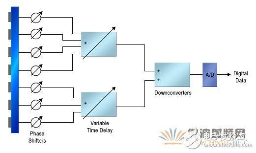
figure 1 . A very simplified diagram of the AESA system structure.
The waveform generator sends the signal to the bunching network. Here, a signal is connected to each transmission channel. At this stage, the digital multiplexer applies amplitude weights on the channel to achieve spatial filtering and shape the waveform. This step can also be done later. In many designs, the signal for each channel is now passed through a digital-to-analog converter (DAC) and then into the analog IF and RF upconverters. After RF upconversion, the signal arrives at a separate transmitter module, with phase shift or delay added, amplitude adjusted (if not done at baseband), and finally filtered and amplified.
In the beginning, the received signal actually passes through the same path as the reverse direction, and more processing is required at the back end. In each antenna unit, a limiter and a bandpass filter protect the low noise amplifier. The amplifier drives an RF downconverter that combines analog amplification and phase modulation. The signal is transmitted from the IF stage to the baseband, and the signal of each antenna unit reaches its analog-to-digital converter (ADC). The bunching module then recombines the antenna signals into one or more complex data sample streams, each data stream representing a signal from a certain receive beam. These signal streams are passed through a large duty cycle digital signal processing (DSP) circuit to further condition the data for Doppler processing, attempting to extract the actual signal from the noise.
When is data conversion?In many designs, most of the signal processing is done in an analog manner. However, as digital speeds increase, power consumption and cost decrease, data converters and antennas are getting closer and closer. Altera application specialist Colman Cheung suggested an ideal system to drive the antenna unit directly from the DAC. However, in 2013, this type of design was not technically possible, especially trans-GHz RF.
It is now possible to place the data converter in the IF for IF frequency conversion, and all baseband processing is digital (Figure 2). The delay of the interference pattern can be generated digitally between the antenna elements in the baseband bunching network, and each antenna element does not require an analog phase shifter or delay line. This partitioning method allows DSP designers to decompose the transmit and receive paths into separate functions—multipliers, filters, FIFOs for delays, and adders, which are modeled in MATLAB and implemented from the library. they. You can put the most demanding functions into a specially developed ASIC, FPGA, or GPU chip, and group less demanding operations into code in a DSP chip or accelerator.
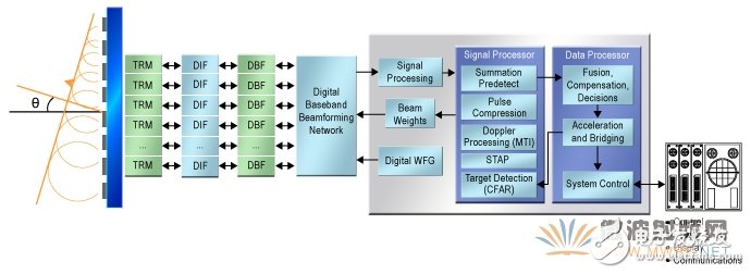
figure 2 . Put the data converter to the end of the IF level.
Special attention needs to be paid to the receive chain signal processing after the signal has come out of the bunching network because its memory and processing requirements are very large and the dynamic range involved is very wide – from the interfering transmitter input to each edge of the search detection range . High-precision floating-point hardware is needed, and more processing power is required.
At its final level, the receiving chain is purposefully modified and implemented. Through its filtering, bunching, and pulse compression stages, the chain's task is to extract signals from noise, especially those that may carry the actual target information in the environment. Then, the focus shifts from the signal to the targets they represent, and the nature of the mission changes.
From signal to targetPulse compression is the beginning of this abstraction process. In the time domain or frequency domain, the pulse compressor generally finds the waveform that may contain the transmitted chirp by autocorrelation. It then uses pulsed targets to represent these waveforms—packets containing arrival time, frequency, and phase, and other related data. From here on, the receiving chain will process this packet instead of the received signal.
The next step is generally Doppler processing. First, the pulse is sent to the grid array (Figure 3). In the array, each column contains pulses that are returned from a certain emitter. There are many columns in the array, depending on how much latency the system can withstand. The rows in the array represent the return switching time: the further away from the x-axis of the array, the greater the delay between the transmitter å•å•¾ and the arrival time of the received pulse. Thus, the delay square also represents the distance from the target reflected by a certain pulse.
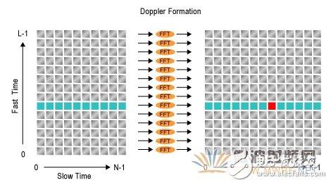
image 3 . Doppler processes the squares.
After placing a series of chirps into the correct square, the Doppler processor moves the data horizontally—observing the change in the pulse returned from a target over time, extracting relative velocity and target header information. This method requires a large ring buffer, and the buffer can hold all the squares regardless of how many squares a Doppler algorithm can process at a time.
Advanced systems add another dimension to the array. By dividing the antenna into sub-arrays, the system can transmit multiple beams simultaneously, and then use the same multiple side-lobe antenna pattern to set the receiver for monitoring. Alternatively, the system scans the beam by focusing or using a synthetic aperture method. Now, when the compressed pulse is loaded, the system creates a three-dimensional grid array: the transmit pulse on one axis, the return delay on the second, and the beam orientation on the third (Figure 4). Now, for each pulse, we have a two-dimensional or three-dimensional grid array that represents both distance and direction—representing physical space. This arrangement of memories is the starting point for Space Time Adaptive Processing (STAP).
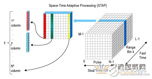
Figure 4 . Multidimensional squares create a matrix for STAP.
This term can be interpreted as: “empty timeâ€, where the data set unifies the position of the target in 3D space and contains the time associated with the target. The reason why it is "adaptive" is because the algorithm obtains adaptive filtering from the data.
Conceptually, the actual situation is also the case. The adaptive filter is a matrix inversion process: Which matrix is ​​this data multiplied to get the hidden result in the noise? According to Michael Parker, senior technical marketing manager at Altera, the hidden pattern information may come from seeds discovered by Doppler processing, data collected from other Sensors, or from intelligent data. An algorithm running downstream of the CPU inserts the hypothesized pattern into the matrix equation and solves the filter function that produces the expected data.
Obviously, at this point, the computational load is very large. The dynamic range required by the inverse transform algorithm requires floating point calculations. For an actual medium-sized system in a combat environment, it must be processed in real time, and Parker estimates that the STAP load will reach several TFLOPS. In systems with low resolution and narrow dynamic range, real-time requirements are not high. For example, a simple car assisted driving system or a synthetic aperture mapping system can significantly reduce this load.
From STAP, the information enters the general-purpose CPU, which is complex but the amount of computation is small. The software tries to classify the target, build the environment model, estimate the threat, or tell the operator, or take immediate emergency measures. At this point, we not only process signals in the signal processing domain, but also enter the field of artificial intelligence.
Two architecturesFrom the perspective of an experienced radar system designer, we are only a superficial understanding of the AESA combat radar. This reference method treats the network as a relatively static DSP chain, both connected to the STA module, which itself is a software-controlled matrix arithmetic unit. In addition, from the perspective of DSP experts, it is a set of CPU cores.
In contrast, automotive or robotic system designers look at the system from a completely different perspective. From an embedded designer's perspective, the system is just a large piece of software, with some very specialized I/O devices and some tasks that need to be accelerated. Experienced radar signal engineers may be dismissive of this approach, given the relative size of signal processing and general-purpose hardware. Clearly, the data rate, flexibility, and dynamic range of the onboard multifunction radar require dedicated DSP pipelines and a large amount of local buffering for real-time processing. But for different applications with several antenna elements, the simple environment, shorter distances, and lower resolution, the CPU-centric view brings some interesting questions.
The first question asked by Professor Gene Frantz of Rice University is to define the real-world I/O. The second problem is choosing the CPU. Frantz notes that “there is very only one CPU. More common is heterogeneous multiprocessing systems.†Frantz suggests that this approach does not start with DSP functions in MATLAB, but begins with a complete system described in C. Then, the CPU-centric designer is not defining the hardware boundary between the DSP and the CPU domain in the design, but “continuously optimizing and accelerating the C code.â€
Actual results may be quite different from DSP-centric approaches. For example, the CPU-centric approach initially assumes that all work is performed on a common CPU. If the speed is not fast enough, this method turns to multiple CPUs, sharing a layered contiguous memory. This approach turns to an optimized hardware accelerator only when multiple cores are not enough to complete the task.
Similarly, a CPU-centric design starts with assuming a unified memory. It allocates a continuous cache for each processor and a local working memory for the accelerator. It does not assume any hardware pipelines at first, nor does it map task mixes to hardware resources.
In the most demanding applications, the same system design may use two architectural approaches simultaneously. The rigorous bandwidth and computational demands of almost every task lead to the use of dedicated hardware pipelines and memory instantiation. Requiring a significant reduction in power consumption may force decisions to adopt high-precision digital methods, which makes it increasingly complicated to share hardware between tasks.
Accuracy is a point that Frantz emphasizes. He pointed out that "halving the effective number of bits allows you to increase performance by an order of magnitude." To reduce power consumption, you can sacrifice or partially sacrifice these.
Frantz pointed out the problem with analog/digital boundaries. He said: "We need to reconsider analog signal processing. Thirty years ago, we started telling system designers that we only need to do data conversion. We use digital methods to do all the other work. But actually, in 8-bit resolution, simulation And the digital method is probably the same. Is the simulation better? It depends on what is the meaning of 'better' in your system."
Narrow-band systems such as geosynthesis or synthetic aperture radar systems used in automated land vehicle systems use a completely different architecture than combat radar. It can use analog filters, upconverters/downconverters, and bunching to perform all subsequent processing of a wideband memory system, as well as multiple heterogeneous processors with floating point accelerators and dynamic load balancing (Figure 5).
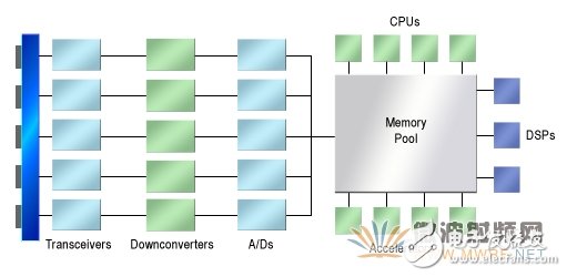
Figure 5 . An ideal low performance AESA system.
Visualizing the signal processing tasks to complete them in software, the system designer gains new runtime choices, such as moving processing resources between tasks, shutting down unwanted processors, and modifying algorithms as early as possible to respond Data pattern, or run multiple algorithms to see which one gives the best results.
The AESA radar system not only provides a rich environment for research implementation strategies, but also provides a way to study systems with a large number of signals. These active arrays are distributed in a variety of design applications such as military, so they should not be limited to traditional embedded design ideas. Therefore, there are new ideas for completely different fields that require a large number of signals, including applications such as signal intelligence and network security. This is a noteworthy area.
By using the SVLEC strain relief systems the user can quickly assemble organize and provide strain relief for cables .The systems can be used for organizing cables in machines , switch cabinets , enclosures and dynamic cable carriers .
With a variety of mounting options, SVL cable relif plate can be used for various cable sizes, and strain relief plate are quick and easy to install, and no installation tools are required
The unique shape allows the cable to be securely held with standard nylon cable ties, and the installation density can be greatly increased by multi-layer installation
cable relif plate,strain relief plate,PA relif plate
Kunshan SVL Electric Co.,Ltd , https://www.svlelectric.com