
Prevent FPGA design from being pirated: cost-effective certification scheme effectively protects SRAM-based FPGA design IP
The application note describes the FPGA (Field Programmable Gate Array) and how to protect the key functions and intellectual property (IP) of the system. This article discusses various ways of IP protection. SHA-1 challenge-response authentication is considered to be the most secure method. This paper presents a cost-effective certification scheme that protects the FPGA design IP based on SRAM. Describes the features of the DS28E01 and DS28CN01 1-Wire devices.
Over the past 20 years, FPGAs (Field Programmable Gate Arrays) have evolved from prototyping tools to flexible solutions for consumer and industrial applications. As FPGA logic complexity increases from thousands of logic gates to millions of logic gates, the device can accommodate more system-critical functions (ie, intellectual property, IP).
Today, designers can choose FPGAs to protect configuration data with a variety of technologies—OTP (one-time programmable) anti-fuse, flash-based reprogrammable memory cells, and reprogrammable, SRAM-based configurable logic cells. Since the configuration data is stored on the FPGA chip, and the chip has a mechanism to prevent stored data from being read, anti-fuse and flash-based solutions both provide relatively safe solutions. In addition, unless very sophisticated methods, such as unpacking, microprobes, voltage contrast electron beam microscopy, and focused ion beam (FIB) detection, are used to "eave" the silicon body and invalidate the security mechanism1, the data is destroyed. The probability is very low (for brief background information on FPGA, please refer to Appendix A, FPGA Technology and Related Matters).
However, FPGAs based on static RAM (SRAM) have almost no security measures to protect IP (configuration data) and prevent data from being illegally copied and plagiarized. The reason is that once the data is loaded, it is stored in the SRAM memory unit, and the memory is easily detected to determine its content. In addition, there is a lack of a certain security mechanism to protect the configuration data before loading into the chip, which opens the door to various detection measures. Since the bitstream is usually stored in a separate memory chip and read by the FPGA in the power-up loading configuration mode, it is possible to traverse the data. Nevertheless, you can find some simple ways to protect data, prevent artificial copying of configuration data, and plagiarism of IP.
In the two-chip solution (FPGA and configuration memory), the configuration data bit stream is exposed to the outside during the power-up phase, and the FPGA cannot distinguish whether the bit stream is "real data" or an illegally obtained copy. The IP contained in the configuration data is completely protected. This problem can be partially solved by key and bitstream encryption. However, due to the high cost of this protection method, it can only be used in high-end FPGAs and is not suitable for consumer products.
Without bitstream encryption, SRAM-based FPGA designs are particularly vulnerable to piracy. The configuration bitstream can be captured and reprogrammed into the configuration PROM, or simply played back to clone the original design. This allows cloned products to compete with original products, steal research and development investment, and reduce the original manufacturer ’s market share and benefits.
Even without encryption, anti-fuse or flash-based FPGAs are more secure than SRAM-based FPGAs because configuration data is not exposed to the outside. However, if the FPGA is programmed by the assembly plant, it is possible for the assembly plant to program and sell more equipment (more than the authorized number) without investing any research and development costs. It is difficult to distinguish such unauthorized devices from authorized devices, which will seriously affect the company's profits.
One way to improve the security of FPGA design based on SRAM to a certain extent is to use multi-chip packaging and package non-volatile memory with FPGA. But if someone opens the package, the data interface between the memory and the FPGA will still be exposed to the outside, and the security of the configuration mode may still be threatened.
The structure of the configuration bit stream (that is, the order of data bits, how to encode and identify) basically has no formal documentation. Although theoretically feasible, the ambiguity, complexity, and size of the bitstream make reverse engineering very difficult and time-consuming1. If the reverse engineering is successful, even if only part of the reverse engineering is performed on the configuration data stream, it is still possible to illegally invade the set-top box to steal services or tamper with the power settings of the vehicle, resulting in the original manufacturer ’s liability.
In order to prevent the system cost from increasing sharply, designers must also continue to use SRAM-based FPGAs without encryption. But they must find a method of IP protection, and control the cost of security measures to the lowest possible level, and will not have a big impact on the production process.
It is very important for the design to install the hardware circuit for safety protection into the space allowed by the circuit board without increasing the overall power consumption. Also, the impact of security on FPGA resources (for example: the number of pins and logic units) must be as small as possible.
The purpose of the authentication process is to establish identity verification between two or more entities. The key-based authentication method takes the key and the data to be verified (ie, "information") as input, and calculates the information verification code (MAC). The MAC is then added to the message, and the receiver of the message performs the same calculation and compares the calculated MAC with the MAC transmitted with the message. If the two MACs are consistent, the information is determined to be reliable.
This basic model has a disadvantage: the intercepted message can be resent by the non-verified sender later and is mistaken for being authenticated. If the MAC calculation includes a random challenge selected by the MAC receiver, the probability of success of this simple "replay attack" will be avoided. Figure 1 shows the general concept of this model. The longer the challenge code, the more difficult it is for potential replay to record all possible responses. 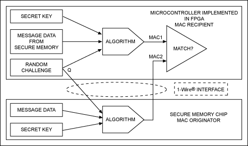
Figure 1. The challenge-response authentication process verifies the authenticity of the MAC sender
To verify the authenticity of the MAC sender, the MAC receiver generates a random number and sends it as a challenge to the sender. Then, the MAC sender must calculate the new MAC based on the key, information, and receiver's challenge. Subsequently, the sender returns the calculation result to the receiver. If the sender is verified to be able to calculate a valid MAC for any challenge code, it can confirm its known password and be considered reliable. This process is called challenge-response authentication (see Figure 1).
There are many algorithms for calculating MAC, such as Gost-Hash, HAS-160, HAVAL, MDC-2, MD2, MD4, MD5, RIPEMD, SHA series, TIger and WHIRLPOOL. After careful consideration and one of the internationally recognized one-way hash algorithms is SHA-1, this algorithm was developed by the National Institute of Standards and Technology (NIST). SHA-1 has been included in the international standard ISO / IEC 10118-3: 2004.
You can query the mathematical basis of the SHA-1 algorithm through the NIST website. The SHA-1 algorithm has the following significant features:
For the above reasons, and the international recognition of the algorithm, SHA-1 has become the best choice for secure memory challenge-response authentication.
Challenge-response authentication schemes can be implemented as part of SRAM-based FPGA system design, which is inexpensive (Figure 2). In this example, the secure memory device is connected to the FPGA pin configured for bidirectional (open drain) communication through only one pin. A resistor connected to VDD powers the safety memory and provides a bias for open-drain communication. Maxim's DS28E01 1Kb protected 1-Wire EEPROM with SHA-1 engine is very suitable for this design. The device contains a SHA-1 engine, 128 bytes of user memory, a key that can be used for internal operation of the chip but cannot be read from the outside, and a unique, unchangeable identification code. 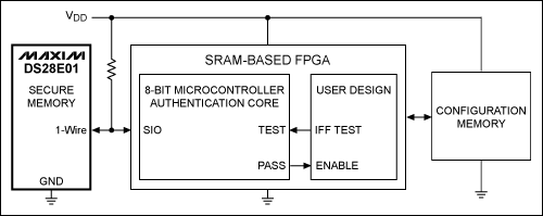
Figure 2. In this simplified block diagram, a 1-Wire secure memory is used to protect the FPGA.
The DS28E01's 1-Wire interface reduces the communication channel to a single FPGA pin for challenge-response authentication. Because FPGA I / O pins are often limited, this security scheme has minimal impact on the system. Another constructable implementation is to use FPGA to implement a general-purpose I²C interface, certification through DS28CN01 (I²C device equivalent to DS28E01), or by implementing SHA-1 engine and other functions in small-scale ASIC or CPLD. However, if security protection is the only function of the device, using ASIC will greatly increase the cost.
In order to strengthen the security features of DS28E01, FPGA must be able to perform the following operations:
For detailed information on SHA-1 MAC calculations, please consult Secure Hash Standard 2.
Some major FPGA vendors provide macros similar to microcontroller functions. The Xilinx® microcontroller function occupies 192 logic cells, which is only 11% of a Spartan®-3 XC3S50 device. Similar microprocessors in Altera® devices occupy 850 logic cells, which is equivalent to 18.5% of EP2C5 (the smallest size of the Cyclone® II series).
At power-up, the FPGA configures itself from its configuration memory. The current FPGA microcontroller function takes effect and performs challenge-response authentication, also known as enemy identification (IFF). This identification process includes the following steps:
Generate a random number and send it as a challenge (Q) to the secure memory. Notify the secure storage to calculate the SHA-1 MAC based on its key, challenge, unique identification code, and other fixed data. Calculate the SHA-1 MAC based on the same input, the constant used by the secure memory, and the FPGA key, which is the expected response (MAC1). The SHA-1 MAC (Read Authentication MAC) calculated by the secure memory is compared as the response (MAC2) with the expected response (MAC1). If MAC1 and MAC2 are consistent, the FPGA recognizes its environment as a "friend" because it obviously knows the key. The FPGA changes to normal operation, activating / executing all functions defined by the configuration code. However, if the two MACs are different, the environment must be considered an "enemy". In this case, the FPGA performs application-related operations instead of working normally.
In addition to the inherent security provided by SHA-1, the main security unit of the above-mentioned IFF authentication process is the key, and neither the secure memory nor the FPGA can read it. And, because the data in the bit stream is messy, when the FPGA configures itself, eavesdropping on the configuration stream will not reveal the key. Considering the size of the data bytes, reverse engineering the bitstream to speculate that the design architecture is very time-consuming and it is almost impossible to complete this task.
Another crucial security measure is the randomness of the challenge. A predictable challenge (constant) produces a predictable response, which can be recorded once and then replayed by a microcontroller that emulates secure memory. Using predictable challenge codes, the microcontroller can successfully let the FPGA recognize it as a "friend." The randomness of the challenge code in the IFF method eliminates the above concerns.
If the key in each secure memory is related to the device, the security can be further improved: each specific key is calculated using the master key, the unique identification code of the SHA-1 memory, and related constants . If a specific individual password is disclosed, it will only affect a single device, not the security of the entire system. To support individual keys, FPGAs need to know the master key and first calculate the key of the 1-Wire SHA-1 memory chip before calculating the expected response.
For all units to be built, the developer (OEM) must provide appropriate pre-programmed secure memory to the contract manufacturer (CM) that manufactures products using embedded FPGAs. This one-to-one relationship limits the number of authorized devices that CM can build. In order to prevent the CM from stealing the secure memory (for example: claiming that some memory needs incorrect programming due to incorrect programming), it is recommended that the OEM set write protection for the security key.
Even if it is not write-protected, there is no need to worry about the safety of the 1-Wire EEPROM data memory. The design ensures that only the person who knows the key can change the memory data. This additional role is very popular because it allows application designers to perform software function management—FPGAs can activate / deactivate certain functions based on data read from SHA-1 secure memory.
OEMs do not always pre-program memory devices before shipping them to CM. To solve this problem, secure memory manufacturers can set up SHA-1 keys and EEPROM array pre-programming services for OEMs. Maxim provides you with such a service, according to the OEM input, register and configure the secure storage at the factory, and then ship it directly to CM. The service has the following main advantages:
The FPGA security certification scheme introduced in this article has been tested on Altera and Xilinx products. Altera concluded in its white paper "An FPGA Design Security SoluTIon Using a Secure Memory Device": "Even if the configuration data bitstream is captured, this FPGA The securely designed IFF scheme can also prevent Altera FPGA designs from being cloned. Only when the calculation results of the hash algorithm of the FPGA and the secure memory are consistent, the user design will be effective. This secure design can effectively protect the FPGA designer ’s IP †3.
Similarly, Xilinx also stated in its application note XAPP780: "The security of the system is based on the security of the key and the loading of the key in a secure environment. The entire reference design, except the key, satisfies the universal The principle of Kerckhoffs. The simple interface for programming and authentication provided by the application notes simplifies the implementation of anti-piracy protection schemes â€4 (Flemish linguist Auguste Kerckhoffs pointed out in his very creative article on the field of military encryption: in addition to relying on ambiguity , Security should rely on the power of the key. He advocates that only the key needs to be replaced when it is compromised, not the entire system).
Simply add a low-cost chip similar to the DS28E01 and update the FPGA configuration code to achieve IP protection and avoid design piracy. With the 1-Wire interface, only one pin of the FPGA needs to be used for security design. If the FPGA has more pins, you can use secure memory with an I²C interface instead of a 1-Wire design. The design also requires some modifications to the FPGA configuration and control software of the embedded microcontroller.
It is possible to order fixed keys or secure storage for calculation keys and special application data. Then send the pre-programmed device only to the OEM, or to the authorized CM. CM can only produce and provide the same number of products as pre-programmed devices.
Five mainstream FPGA vendors—Actel®, Altera, LatTIce Semiconductor CorporaTIon®, QuickLogic®, and Xilinx—have nearly 98% market share. The remaining 2% share belongs to several special vendors that provide similar FPGA functions.
All these manufacturers adopt outsourcing operation mode and rely on wafer processing plants in Taiwan, Japan, Singapore or Germany to produce chips for them. Therefore, they only have the authority to operate the technical parts related to their factories, such as the use of SRAM functions or fast logic of high-density floating gate memory arrays. By giving full play to the role of standard processing procedures, FPGA companies can keep their manufacturing costs very low.
However, Actel and QuickLogic and their processing plants have integrated intellectual property anti-fuse technology into the processing flow. Anti-fuse technology has some unique advantages: good security, small cells, radiation resistance, and of course non-volatility. Anti-fuse technology has a limitation. Unlike flash-based devices, once a cell is configured, it cannot be reconfigured (as the literal meaning of "fuse"). In addition, although the anti-fuse process is more complex than SRAM-based FPGAs, its cells are smaller, resulting in smaller chips with logic capabilities and lower costs.
For a long time, SRAM and flash memory technologies were mutually exclusive; they could not be easily integrated into one chip. But this situation has changed, due to the recent market demand to promote the development of semiconductor technology. Small competitors (Actel, Lattice Semiconductor, and QuickLogic) now offer single-chip flash-based FPGAs (ProASIC, Lattice® XP2, and PolarPro, respectively).
For example, since 2004, Altera has begun to provide flash-based CPLD (MAXII), but currently does not apply this technology to FPGA. Xilinx launched the Spartan-3AN production line of flash-based FPGAs back in 2007, with two chips (FPGA and flash) installed in a single package. But Xilinx does not have a single-chip flash-based FPGA product5. The ability to integrate flash memory facilitates the improvement of IP security using external configuration memory through SRAM-based FPGAs. By integrating on one chip, it is more difficult to plagiarize the data transferred between the memory and the configurable logic array.
One way to meet all these security requirements is to use challenge-response data exchange (authentication) between the FPGA and the secure memory. The secure memory chip was invented in the late 1980s. They were first widely used with payphone cards, and then were applied to bank cards in the 1890s; today they are an important part of GSM mobile phones (ie SIM cards). The common communication standard between the secure chip card and the host system is the I²C serial bus.
Whether it is tailored for banking or telephone applications, secure storage is not feasible for general purposes. This situation changed when Dallas Semiconductor (now Maxim Integrated Products) introduced devices incorporating SHA-1 hashing algorithms in 2000. Following the first generation of DS2432, an enhanced DS28E01 was introduced. These devices use a 1-Wire interface for communication and power supply. The DS28CN01 introduced in 2007 uses an I²C interface, and is similar to the DS28E01 in other respects.
Since processing plants often have detailed knowledge of FPGA design, another aspect to consider regarding IP security is the integrity of the processing plant. In order to prevent the theft of ownership information, trust or strict control and supervision are necessary. This is easier for domestic processing plants than for foreign processing plants. Nonetheless, to date, the major processing plants have demonstrated excellent integrity in terms of safety design details.
AA/AAA battery is 1.5V lithium battery with high capcacity, the cycle life is more than 1000 times, 1-2 hours can be fully charged. USB charging, one set with the battery box can be a charger.
Self-discharge small, good battery, under 2% per month (recoverable). No memory effect. The operating temperature range is -20℃ ~ 60℃. Excellent cycle performance, fast charging and discharging, charging efficiency up to 100%, and large output power. Long service life. It does not contain poisonous and harmful substances and is called green battery.
Best Rechargeable Batteries,Rechargeable Battery Cell,Rechargeable Lithium Batteries,Rechargeable Lithium Battery,Environmentally Friendly ,1.5v Battery Backup
Shenzhen Enershare Technology Co.,Ltd , https://www.enersharepower.com