
Powering digital image sensors in automotive camera applications involves a variety of different design elements. High levels of image quality are essential in rainy, snowy, foggy and other difficult driving environments. The driver of the car relies heavily on the technology when reversing. If the main design elements of the analog power rail's low noise requirements, efficiency and size cannot be optimized, then a well-functioning solution in good weather conditions may not be suitable for harsh weather conditions.
This article refers to the address: http://
Design element
Powering digital image sensors in automotive camera applications involves a variety of different design elements. Image quality is an important indicator of whether such applications are profitable. High levels of image quality are essential in rainy, snowy, foggy and other difficult driving environments. The driver of the car relies heavily on the technology when reversing. If the main design elements of the analog power rail's low noise requirements, efficiency, and size are not optimized, a well-functioning solution in good weather conditions may not be suitable for harsh weather conditions.
Advanced driver assistance system
For example, the AptinaAR0132 is a popular sensor with 1.2 megapixels and 720p60 resolution for high dynamic range imaging for automotive advanced driver assistance (ADAS) and surround view/parking assisted camera applications. The core (VDD) and I/O sections (VDD_IO) require 1.8V, and the analog sections (VAA, VAA_PIX, and VDD_PLL) require 2.8V. Obviously, the analog portion of the chip is more susceptible to its power line noise. Many designs use a low dropout regulator (LDO) to downconvert all power from the 5V input rail.
Design goals
The overall goal is to provide a practical power system implementation for the AR0132AT image sensor, enabling its successful integration into automotive applications and packaging. While the details of other sensors and systems may vary, the principles discussed in this article have general applicability.
The size of the image sensor is very important because it must be incorporated into a 25 mm cube, which puts high demands on overall efficiency and good thermal management. Although the LDO has a low-noise output, its high power consumption can cause adverse effects on the image sensor, so it is not ideal for working in a 25 mm cube.
Switching power solutions consume much less power, but inherently have higher output ripple and noise. When implementing a switching power supply solution, additional attention needs to be paid to the noise (ripple) sensitivity of the image sensor to its analog input power rail.
designing process
In order to design a power system that can efficiently supply image sensors, it is necessary to know the sensor sensitivity level and the ripple output of the switching power supply in order to take appropriate design steps to reduce the ripple on the sensor supply rail below the degradation threshold.
Image sensor noise threshold measurement
The simple circuit in Figure 1 is used to define the noise threshold for each sensor power rail.
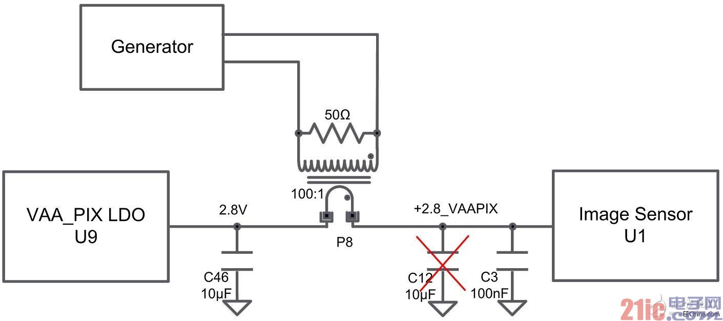
Figure 1 noise threshold test circuit
By observing the image quality with the Aptina Devware development software running on a laptop, we saw that the generator frequency was increased from 50 kHz to 5 MHz. In the case of sensitive orbits, the signal size will continue to diminish until visual artifacts no longer appear.
Component selection considerations
Since the overall power requirements are very low (digital core/input and output is 0.28W, analog part is 0.42W), we must select a power conversion IC with a rated input operating voltage of 13.5V and high efficiency operation at low output current. Based on these factors, we should choose a constant time (COT) architecture. The COT architecture is ideal for applications that operate efficiently under light loads and that achieve good load transient response with minimal external current capability. Achieving high efficiency at light loads results in more output ripple, similar to the Pulse Frequency Modulation (PFM) mode scheme. The COT architecture can help in two areas: efficiency/thermal management and solution size.
Selecting components that can withstand load dump voltages (typically 40V) in automotive applications has the great advantage of helping to minimize or eliminate input protection circuitry.
Power architecture
Since the sensor is designed to meet the needs of the automotive environment, we should naturally choose the LM34919C as an example. With an input voltage range of 4.5V to 50V, the device is ideal for automotive battery-powered applications.
The LM34919 front-end not only provides 2.8V for the AR0132 directly from a 12V automotive battery, but also provides input to the LM3671 1.8V regulator.
Figure 2 shows the overall power architecture of the design example.
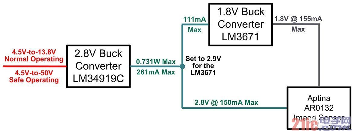
Figure 2 overall power architecture
Meet the noise threshold requirements of image sensors
The LM34919C's constant time architecture requires a minimum of 25mVP-P ripple on the FB pin to maintain the desired stability. The design requirements of the LM34919 are exactly the opposite of the design intent to reduce the ripple voltage of the image sensor's sensitive rails.
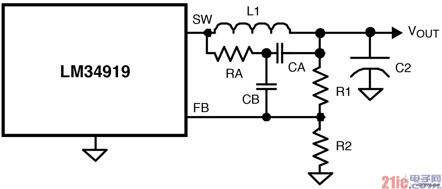
Figure 3 Minimum Output Ripple Circuit
To minimize output ripple while maintaining reliable stability, we used the ripple rejection circuit in Figure 3. This circuit not only provides sufficient ripple to the FB pin, but also reduces the ripple at the output below 10mVP-P.
To further prevent image artifacts from ripple, an RC filter can be used to protect sensitive rails. In addition to providing proper ripple attenuation, RC filters are primarily designed to achieve the lowest power consumption. Although only the VAA and VAA_PIX rails show sensitive characteristics during the test, the VDD_PLL rail (Figure 4) can be filtered, just in case.
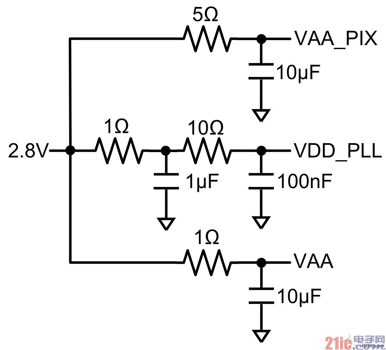
Figure 4 RC ripple filter
All three supplies achieved a target attenuation of 40db around 2MHz (Figure 5). This reduces the image sensor ripple to 100μV, which is 40db lower than any sensor noise threshold observed.
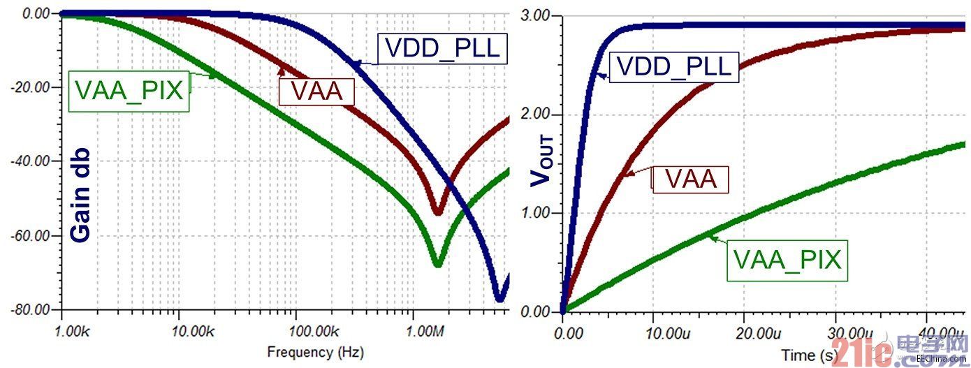
Figure 5 RC filter frequency and transient response simulation
To meet the PLL power-first AR0132AT power sequencing requirements, the VDD_PLL power supply uses a two-pole filter.
In each instance, the last filter capacitor of each power supply is doubled with the input bypass of the image sensor.
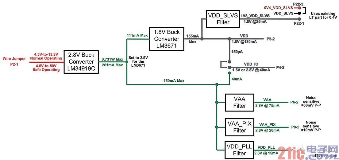
Figure 6 Block diagram of the final power system
For ease of testing, the power supply system implements a daughter card setup that plugs into the pinholes on the AR0132 demo front panel (originally LDOs for all rail voltages). Among them, unused linear regulators and other components are removed. This combination is primarily used to demonstrate image quality and the performance of alternative power systems.
LED garden light,High Quality LED garden light,LED garden light Details, CN
ZHONGSHAN G-LIGHTS LIGHTING CO., LTD. , https://www.glightsled.com