
Switching power supplies have been widely used for their high efficiency and small size. Conventional switching power supplies generally use voltage-type pulse width modulation (PWM) technology, and in recent years, current-mode PWM technology has developed rapidly. Compared with voltage-type PWM, current-mode PWM has better voltage regulation and load regulation, and the stability and dynamic characteristics of the system are also significantly improved. In particular, its inherent current limiting capability and parallel current sharing capability make the control circuit change. It is simple and reliable.
The current-type PWM integrated controller has been commercialized, which greatly promotes the development and application of small-power switching power supplies. The current-mode PWM control low-power power supply has replaced the voltage-type PWM control low-power power supply. Unitrode's UC3842 series of control chips are typical representatives of current-mode PWM controllers.
DC/DC converter
The converter is one of the most important components of a switching power supply. It has five basic types: single-ended forward, single-ended flyback, push-pull, half-bridge, and full-bridge converters. The following analysis focuses on the isolated single-ended flyback converter circuit. The circuit structure is shown in Figure 1.
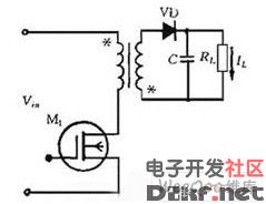
Figure 1 circuit structure diagram
The circuit works as follows: When M1 is turned on, it stores energy in the primary inductor of the transformer, and the diode VD connected to the secondary of the transformer is in a reverse bias state, so the diode VD is turned off, and no current flows through the secondary of the transformer, that is, No energy is transferred to the load; when M1 is turned off, the polarity of the voltage in the secondary inductor of the transformer is reversed, causing VD to conduct, charging the output capacitor C, and there is also a current I flowing through the load R. The equivalent topology of M1 conduction and cutoff is shown in Figure 2.
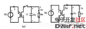
Figure 2 Equivalent topology of M1 conduction and cutoff
Current mode PWM
Compared with the voltage-type PWM, the current-mode PWM control adds an inductor current feedback link in addition to the output voltage feedback control, and uses this current feedback as a ramp function necessary for the PWM.
The following is an analysis of the operation of a current-mode PWM circuit under ideal no-load (without considering mutual inductance). The circuit is shown in Figure 3. Let V turn on, then
L·diL/dt = ui (1) iL increases linearly with slope ui/L, and L is the primary inductance of T1. The non-inductive resistor R1 samples Ud=R1·iL to the pulse width comparator A2 and Ue. When Ud>Ue, A2 outputs a high level and is sent to the reset end of the RS latch. There must be a high level in each input, and the power switch tube V is turned off after the NOR gate output. When the clock output is high, the NOR gate output is always low, blocking PWM, this time is determined by the clock width of the clock oscillator OSC output, that is, the dead time of the PWM signal. While the oscillator output pulse drops, both the NAND gate inputs are low, and the NAND gate output is high and V is turned on.
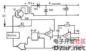
Figure 3 Current-mode PWM circuit under ideal no load
In short, the rising edge of the PWM signal is determined by the falling edge of the oscillator, and the falling edge of the PWM is determined by the inductor current limit signal and the error signal Ue. The falling edge of the maximum pulse width is controlled by the rising edge of the oscillator. Figure 4 is a timing diagram of its operation.
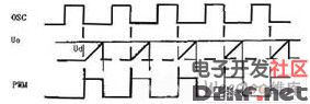
Figure 4 working sequence diagram
Introduction to UC3842 (Click to view: UC3842A UC3843A Chinese information)
Unitrode's UC3842 is a high performance fixed frequency current type controller that includes an error amplifier, PWM comparator, PWM latch, oscillator, internal reference power supply and undervoltage lockout. The structure is shown in Figure 5. .
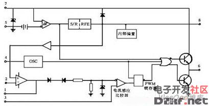
Figure 5 UC3842 structure diagram
The function of each pin is as follows.
The 1-pin COMP is the output of the internal error amplifier. Usually a feedback network is connected between this pin and pin 2 to determine the gain and frequency response of the error amplifier.
The 2-pin FEED BACK is the feedback voltage input. This pin is compared with the reference voltage of the internal error amplifier's non-inverting input (typically +2.5V) to generate the control voltage and control the pulse width.
The 3-pin ISENSE is the current sensing terminal. In the peripheral circuit, a small resistance value sampling resistor is connected in series with the source of the power switch tube (such as the VMos tube), and the current of the pulse transformer is converted into a voltage, which is sent to the pin 3 to control the pulse width. In addition, when the power supply voltage is abnormal, the current of the power switch tube increases. When the voltage on the sampling resistor exceeds 1V, the UC3842 stops outputting, effectively protecting the power switch tube.
The 4-pin RT/CT is the timing terminal. The sawtooth oscillator externally connects the timing capacitor C and the common terminal of the timing resistor R.
The 5-pin GND is grounded.
The 6-pin OUT is the output. This pin is a Tuen-style output with a drive capability of ±1A. This totem pole structure is advantageous for the shutdown of the driven power tube, because when the triode VTl is turned off, VT2 is turned on, providing a low impedance reverse current loop for the power tube to turn off, and accelerating the power tube to turn off. .
The 7-pin Vcc is the power supply. When the supply voltage is lower than +16V, the UC3824 does not work, and the power consumption is below 1mA. The input voltage can be obtained from a high voltage step-down through a large value resistor. After the chip is working, the input voltage can fluctuate between +10 and +30V, and stop working below +10V. The power consumption is about 15mA during operation, and this current can be supplied through a feedback resistor.
8-pin VREF is the reference voltage output that outputs an accurate +5V reference voltage up to 50
mA.
The UV3842 voltage regulation rate can reach 0.01%, the operating frequency is 500kHz, the starting current is less than 1mA, the input voltage is 10~30V, the reference voltage is 4.9~5.1V, the working temperature is 0~70°C, and the output current is 1A.
Switching power supply
The switching power supply circuit composed of UC3842 is shown in Fig. 6, and T is a high frequency transformer. Just after power-on, 220V AC first filters out RF interference through PNF, and then rectifies and filters to obtain about +300V DC voltage, and then R22 steps down to provide +16V startup voltage to UC3842. R1 is a current limiting resistor and C1 is a filter capacitor. After normal operation, the high-frequency voltage on the self-feeding coil N2 is rectified and filtered by VD1 and C1, which is used as the normal working voltage of the UC3842. R5 and C4 are used to improve the frequency response of the internal error amplifier, and R1 is the slope compensation resistor. On-off level. C5 is the noise canceling capacitor, R10 is the overcurrent detecting resistor, and R7 is the gate current limiting resistor of the VMOS switching power tube. A two-stage absorption loop is formed by C8, VD1, R11, VD2, and C9 for absorbing the peak voltage. VD1 and VD3 use recovery diode FR305. VD4 is the output stage rectifier, using Schottky diodes to meet the needs of high frequency, high current rectification.
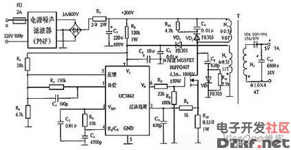
Figure 6 UC3842 switching power supply circuit
When the NMOS transistor is turned on, the current of the primary winding N1 increases linearly, the magnetic field is enhanced, and the VD4 in the secondary coil is turned off, and the capacitor C10 supplies power to the load; at this time, the VD2 in the primary loop of the pulse transformer is also cut off, and N1 is stored at this time. The role of energy. When the NMOS transistor is turned off, the primary coil current decreases, the magnetic field is weakened, VD4 in the secondary coil loop is turned on, energy is released to the load through VD4 and C10, and a DC voltage is output, and part of the energy is released from VD2 to the resistor R12 and the capacitor C9.
In order to ensure that the switching power supply output DC voltage is not disturbed, a voltage stabilization circuit is provided in the circuit. First, the NMOS tube source series resistor R9 is used to change the current signal into a voltage signal, and the UC3842 is fed as a comparison voltage to control the duty cycle of the excitation pulse to achieve the purpose of voltage regulation. Second, the coil N2 in the transformer T is indirectly sampled and acts as a voltage feedback. After indirect sampling by N2, it is rectified by VD1 and C3, and sampled on C3. The voltage is divided by R3 and R4 and sent to the 2 pins of UC3842. It is applied to the inverting input of error amplifier A3, and directly to the 7 pin of UC3842 as the chip supply voltage. When the circuit is started, the input voltage is stepped down by the rectification filter to supply power to the chip. After the operation, the voltage is supplied by the feedback voltage. Therefore, the power supply voltage of the UC3842 reflects the change of the output voltage and plays a feedback role to stabilize the output voltage. Third, in UC3842, the slope of the output sawtooth wave of the sawtooth generator is also related to the input voltage. When the input voltage rises, the slope of the sawtooth wave increases, and the duty cycle of the output excitation pulse decreases, so that the output voltage remains stable. Vice versa, it is actually equivalent to feedback control.
to sum up
UC3842 is a popular current-type PWM signal generator with high precision, stable voltage, simple peripheral circuit and low price. It is widely used in small power switching power supply with output voltage range of 4.9~5.1V and power of 20~60W. in.
Perfect fit: The Hydrogel Screen Protector is designed with a Soft TPU material, which can be completely covered even on a curved device, providing perfect protection for the full coverage of the screen.
Oleophobic and waterproof: The use of hydrophobic and oleophobic screen coatings can prevent sweat, grease residue and fingerprints without reducing screen sensitivity. It is almost invisible on the screen and brings a high-definition visual experience.
Sensitive touch: ultra-thin and Soft Hydrogel Film with a thickness of only 0.14mm. As time goes by, it will self-repair minor scratches, provide you with a highly responsive screen protector and maintain the original touch.
Easy to install: The installation of the Protective Film is very simple, without air bubbles. The protective sticker can stay on the phone perfectly, and the bubbles will disappear within 24 hours.
If you want to know more about Hydrogel Screen Protector products, please click the product details to view the parameters, models, pictures, prices and other information about Hydrogel Screen Protective Film.
Whether you are a group or an individual, we will try our best to provide you with accurate and comprehensive information about the Hydrogel Protective Film!
Hydrogel TPU Protective Film,Ultra-Thin Protective Film,Soft Hydrogel Film,Hydrogel Film Screen Protector,Screen Protective Film,Mobile Phone Screen Guards
Shenzhen Jianjiantong Technology Co., Ltd. , https://www.jonsun-sz.com