
Integration has always been the key to advances in wireless communications, enabling devices to be versatile and miniaturized. While mobile phones are at the forefront of these trends, lowering costs and accelerating time-to-market are also driving forces for higher levels of cellular infrastructure. As wireless integrated designers strive to integrate more features in smaller packages, higher levels of integration in analog, digital, and high-frequency functions in a single device remain the mainstream trend for ICs. The problem of handset and infrastructure designers trying to integrate multiple wireless standards into a single system complicates the problem. To balance these diverse needs, innovative design techniques leverage the advanced technical resources and expertise of amplifiers, transceivers, and other devices to create systems that are more sacrificial and more integrated.
According to Dale Wilson, senior marketing manager for the RF Division at Analog Devices (ADI), "Size is an important consideration in design, especially in handheld and portable applications; in larger systems, size is also required. Customers want to achieve more and more functions within a certain volume. In most cases, customers want a single device to have multiple functions while reducing costs. In addition, they also hope to reduce assembly and testing costs and simplify Practical design work. If tuning, filtering, biasing, etc. can be implemented on the chip, the workload of the user can be greatly reduced, and the time to market of the customer's products can also be accelerated. The performance of discrete RF components is usually better than that of highly integrated devices. It's better. But in many applications, as long as the target price is achieved, the performance 'good enough' is acceptable. Because analog and high-performance RF devices are more CMOS-based, there are more opportunities to integrate digital control functions."
To meet this high level of integration, Analog Devices has traditionally implemented its advanced bipolar process for its many high performance RF products. The customer then uses digital control within their system. Wilson pointed out that ADI is now using the latest BiCMOS process, which has superior analog performance and the ability to integrate digital control functions into the chip. The CMOS process is also used to implement highly integrated RF devices and uses digital processing to overcome RF performance limitations.
Last fall, ADI first introduced RF mixers and modulators that support high-density RF cards, and it boosts the capacity and speed of Long Term Evolution (LTE) and fourth-generation (4G) base stations (Figure 1). The ADRF670x family of mixers and the ADRF660x family of modulators integrate multiple independent function blocks in a single device. An active RF mixer, single-ended 50-ohm input RF input balun, and a voltage-integrated voltage-controlled oscillator (VCO) are integrated into the product package of the four ADRF660x families. Phase loop (PLL) frequency synthesizer. The active mixer provides 6dB of voltage conversion gain. The differential IF output operates at 500MHz. The ADRF6601 receive mixer operates from 300 to 2500 MHz and the internal LO range is 750 to 1160 MHz. At 12dBm input power, it achieves 1dB of compression and can achieve an input third-order intercept of 30dBm. The single sideband (SSB) noise of this mixer is 12dB.
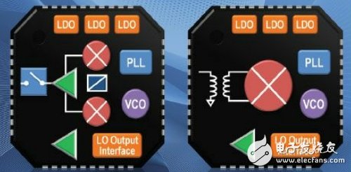
Figure 1: The RF modulator and downconverter include an integrated PLL, a multimode N-times synthesizer that supports LTE 100KHz channel rasters.
Each ADRF670x modulator integrates an analog in-phase/quadrature (I/Q) modulator, an RF output switch, and a phase-locked loop with a voltage-controlled oscillator in the RF IC. The modulator input bandwidth is 500MHz. The PLL/synthesizer of the ADRF6701 I/Q modulator uses a divide-by-F (fracTIonal-N) PLL that multiplies the LO signal and feeds it to the I/Q modulator. The reference input of the PLL accepts signals from 12MHz to 160MHz. The output frequency of the modulator is 400 to 1300 MHz. Its internal L0 frequency range is 750 to 1160 MHz. The device provides 14dBm of output power at a 1dB compression point and a 29dBm output third-order intercept, and provides a noise floor of 158dBm/Hz.
Integration requirements for PAAs 3G wireless networks mature and gradually transition to 4G systems, the use of distributed architectures and active antenna systems is driving the need for smaller, more efficient transceivers and PAs. For example, Maxim's MAX9947 promises to simplify the implementation of base station and tower mounting equipment (Figure 2) that meets the Antenna Interface Standards Organization (AISG). The 3x3mm, single-chip transceiver in TQFN form factor includes a transmitter, receiver and active filter.
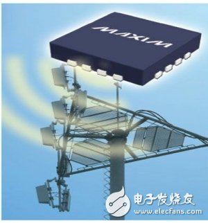
Figure 2: The transceiver integrates an output with AutodirecTIon function that can be used to handle bus arbitration for tower-mounted devices without the need for an MCU.
The transmitter includes an OOK modulator, a bandpass filter that conforms to the AISG spectral emission specification, and an output amplifier. The receiver includes a bandpass filter with a center frequency of 2.176 MHz and a bandwidth of 200 kHz. It also includes a comparator and OOK demodulator for reconstructing the digital signal. With a 50Ω input impedance, the MAX9947 has an input dynamic range of -15 to +5dBm. It can compensate for external circuit and line losses by resistor-regulated output power (7 to 12 dBm). The transceiver supports all AISG data rates: 9.6, 38.4 and 115.2 kb/s.
Usb Cables,Usb Wires,Usb Wire,Micro Usb Cable
UCOAX , https://www.ucoax.com