CPS-SPWM technology is widely used in cascaded H-bridge multi-level converters due to its excellent equivalent switching frequency, small output voltage harmonic content, wide signal transmission bandwidth and simple control method.
The typical SPWM implementation methods are mainly divided into two categories: natural sampling method and regular sampling method. However, the regular sampling method usually has two methods: symmetric rule sampling and asymmetric rule sampling. The paper proposes a GPS-SPWM implementation method based on asymmetric rule sampling method. The conclusion is that compared with the regular sampling method, the sampling point and the calculation amount are doubled; but the output voltage harmonic content of the converter is greatly reduced, and the waveform is greatly reduced. The asymmetry has also improved.
The CPS-PWM pulse generation timing of the cascaded H-bridge multilevel converter is described here. On this basis, a fast and accurate generation method of CPS-SPWM trigger pulse based on asymmetric rule sampling is proposed. The implementation method of CPS-PWM trigger pulse fast generation based on FPGA-based cascaded H-bridge multi-level converter is introduced.
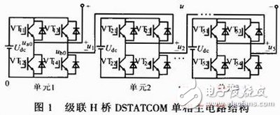
2 CPS-SPWM trigger pulse generation timingThe single-phase main circuit structure of the cascaded H-bridge multi-level converter is shown in Figure 1. For the convenience of analysis, the number of cascaded units is N=5. Yuan left and right arm upper and lower IGBT switching devices; ux is the AC side output voltage of each unit; u is the single-phase output total voltage of the cascading device; Udc is the DC side voltage of each unit. The device adopts a unipolar switching modulation method based on CPS-SPWM, and each unit carrier urx is shifted from each other by time Ts=Tc/(2N), where Tc is a carrier period.

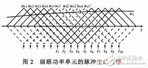
The pulse generation timing of each unit is shown in Fig. 2. The phase of urx is 180° out of phase with urx-, which is used to form the trigger pulses of VTx1 and VTx4 of power unit x, respectively; us is the SPWM modulated wave.

As shown in the figure, the modulated wave us is sampled at time tn (n=1,...,10; Ts is a sampling period, tk+1-tk=Ts), and SPWM trigger pulses Px1, Px4 are sequentially generated according to different sampling methods. Corresponding to triggering VTx1 and VTx4 respectively; VTx2, VTx3 trigger pulses Px2, Px3 are opposite to Px1, Px4, respectively, and the deadband delay is added in practical applications.
In practical applications, the carrier does not exist as a specific waveform, but instead is a bidirectional counter. Here, the counters Tx1 and Tx4 are defined to correspond to the carriers urx and urx-, respectively; Tx1CMP and Tx4CMP are respectively set as the comparison registers of Tx1 and Tx4, respectively.
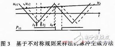
The asymmetric rule sampling method refers to sampling the modulated waves at the peaks and valleys in one carrier cycle, as shown in FIG. Sampling us at t1, calculating the duty cycle and loading it to T11CMP, starting at T2, T11 starts counting up, forming a falling edge of P11 when the comparison is matched; sampling us again at time t6, calculating the duty cycle and updating T11CMP, at T11 The overflow time begins to count down, and when the comparison matches, the rising edge of the next pulse of P11 is formed.

It can be seen that the trigger pulse generated by this method is only one Ts compared with the theoretical pulse delay, and the accuracy is higher because the sinusoidal modulated wave is sampled twice in one carrier cycle. The main disadvantage of this method is that it increases the sampling frequency and increases the computational workload. However, for the trigger timing of the cascaded power unit as shown in FIG. 2, the method neither increases the sampling frequency nor increases the calculation amount, and the specific analysis is as follows:
According to FIG. 3, for generating the same trigger pulse, such as P11, sampling is performed at times t1 and t6, respectively, and the sampling frequency of the pulse generation is twice as high as that of the symmetric regular sampling method. However, in actuality, referring to the cascading unit pulse generation timing shown in FIG. 2, the time t6 also corresponds to the sampling time generated by the trigger pulse P14. Therefore, overall, the sampling frequency is not improved, but only two duty cycles are required at the same sampling time. For the calculation of the ratio, for example, at time t6, calculate the duty ratios D14 and D11 of P14 and P11, respectively. As long as it is proved that D14 is equal to D11 at this time, it means that the method does not need to increase the calculation amount, which proves as follows: TW11=D11Tc, TW14=D14Tc, obviously: (Tc-TW11)/2=(Tc-TW14)/2, the solution is TW11=TW14, that is, D11=D14, it can be seen that only one duty cycle calculation is needed at any sampling time without adding additional calculation amount.
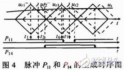
The generation process and timing of P11 and P14 are as shown in Fig. 4. At time t1, sample us and calculate D11 (D14), and load it to T11CMP and T14CMP. When the next synchronization signal arrives, that is, t2 clears T11 and starts counting up, generating the falling edge of P11. At the same time, it reloads T14 and starts counting down. , generates a rising edge of P14. Similarly, at time t6, the sampling us calculates D14 (D11), and loads it to T14CMP and T11CMP. At time t7, it clears T14 and starts incrementing. It reloads T11 and starts counting down, generating the falling edge of P14 and the rising of P11. along.

Referring to Figure 2, the pulse generation timing of the entire cascade unit is:
The SPWM trigger pulses generated by sampling at 1t1, t2, t3, t4, and t5 are: P11↓ (falling edge) and P14↑ (rising edge), P21↓ and P24↑, P31↓ and P34↑, P41↓ and P44↑ , P51↓ and P54↑;
The SPWM trigger pulses generated by sampling at 2t6, t7, t8, t9, and t10 are: P14↓ and P11↑, P24↓ and P21↑, P34↓ and P31↑, P44↓ and P41↑, P54↓ and P51↑.
7.5 Mm Nano Tip,Smart Pen Infrared,Infrared Pen Touch,Slim Infrared Pen
Shenzhen Ruidian Technology CO., Ltd , https://www.wisonens.com
