
RF circuit layouts need to be creative by RF engineers in order to reduce spurious signals. Keeping in mind these eight rules will not only help speed time to market, but also improve the predictability of your work schedule.
Rule 1: The ground via should be located at the ground reference switch
All current flowing through the route being routed has equal reflow. There are many coupling strategies, but the reflow typically flows through an adjacent ground plane or ground that is placed in parallel with the signal line. As the reference layer continues, all coupling is limited to the transmission line and everything is fine. However, if the signal line is switched from the top layer to the inner or bottom layer, the reflow must also obtain the path.
Figure 1 is an example. The top signal line current is immediately below the return current. When it is transferred to the bottom layer, the reflow passes through the nearby via. However, if there are no vias for reflow in the vicinity, the reflow will pass through the nearest available ground via. Farther distances create current loops that form inductors. If this unnecessary current path is offset and happens to cross another line, the interference is more severe. This current loop is actually equivalent to forming an antenna!
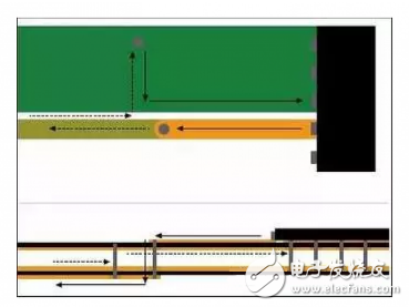
Figure 1: Signal current flows from the device pins through the via to the lower layer. The reflow is below the signal before being forced to flow to the nearest via to the nearest via.
Ground reference is the best strategy, but high speed lines can sometimes be placed on the internal layer. It is very difficult to place the ground reference layer up and down. Semiconductor manufacturers may be pin-limited and place the power line next to the high-speed line. If the reference current needs to be switched between layers or networks that are not DC-coupled, the decoupling capacitor should be placed next to the switch point.
Rule 2: Connect the device pads to the top ground
Many devices use a thermal ground pad on the bottom of the device package. On RF devices, these are typically electrically grounded, while adjacent pad points have an array of ground vias. The device pad can be connected directly to the ground pin and connected to any copper via the top ground. If there are multiple paths, the reflow will be split according to the path impedance ratio. The ground connection through the pad is shorter and the impedance is lower relative to the pin ground.
A good electrical connection between the board and the device pads is critical. Unpacked vias in the via array of the board may also draw away solder paste from the device during assembly, leaving a void. Filling the through holes is a good way to ensure that the welds are in place.
In the evaluation, the solder mask layer was also opened to confirm that no solder mask was on the board ground below the device because the solder mask might raise the device or cause it to sway.
Rule 3: No reference layer gap
Through holes are everywhere around the device. The power network is decoupled and then decoupled and then dropped to the power plane. Typically, multiple vias are provided to minimize inductance and increase current carrying capacity while the control bus can be reduced to the inner layer. All of these decompositions are eventually completely clamped near the device.
Each of these vias creates a forbidden region on the inner ground plane that is larger than the via diameter itself, providing a manufacturing void. These forbidden zones can easily cause interruptions in the return path. Some vias are close to each other to form a ground plane trench, and the top CAD view is invisible, which further complicates the situation. The ground plane voids of the two power plane vias of FIG. 2 can create overlapping forbidden regions and cause an interruption in the return path. Reflow can only bypass the grounding layer forbidden zone, forming a common emission sensing path problem.
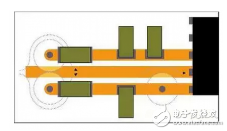
Figure 2: The forbidden areas of the ground plane around the via may overlap, forcing the return to drift away from the signal path. Even if there is no overlap, the forbidden zone will form a rat bite impedance interruption at the ground plane.
Even "friendly" ground vias will bring the minimum size required for board manufacturing processes to the associated metal pads. If the through hole is very close to the signal line, it will have the same erosion as if the top grounded space was bitten by the mouse. Figure 2 is a schematic view of a rat bite.
Since the forbidden area is automatically generated by the CAD software and the through hole is used frequently on the system board, there are almost always some return path interruption problems in the initial layout process. Track each high-speed line during layout evaluation and check the relevant reflow layer to avoid interruption. It is a good idea to have all vias that can create ground plane interference in any area closer to the top ground gap.
Rule 4: Maintain differentiality of differential lines
The return path is critical to signal line performance and should be considered part of the signal path. At the same time, differential pairs are usually not tightly coupled and reflow may flow through adjacent layers. Both reflows must be routed through equal electrical paths.
Even if the two lines of the differential pair are not tightly coupled, the adjacent and shared design constraints will cause the reflow to be at the same level. To really keep the parasitic signal low, a better match is needed. Any planned structure, such as a current interrupter under the differential component, should be symmetrical. Similarly, a length match may also create a waveform curve problem in the signal line. Reflow does not cause waveform problems. The length matching of a differential line should be reflected in other differential lines.
Rule 5: No clock or control line near the RF signal line
Clocks and control lines can sometimes be seen as neighbors that have no effect because they work at low speeds, even close to DC. However, its switching characteristics are almost square waves, producing unique tones at odd harmonic frequencies. Although the basic frequency of square wave emission energy will not have any effect, its sharp edge may have an impact. In digital system design, the corner frequency estimates the highest frequency harmonic that must be considered, calculated as: Fknee = 0.5 / Tr, where Tr is the rise time. Note that it is the rise time, not the signal frequency. However, square waves with sharp edges also have strong high-order odd harmonics that may only drop at the wrong frequency and couple to the RF line, violating strict transmission mask requirements.
The clock and control lines should be isolated from the RF signal line by an internal ground plane or a ground pour. If grounded isolation signals are not available, the wiring should be ensured at right angles. Because the flux lines emitted by the clock or control line form a radiating cylindrical contour around the currents that interfere with the source line, they will not generate current in the receiver line. Slowing the rise time not only reduces the corner frequency, but also helps reduce interference from the source of interference, but the clock or control line can also act as a receiver line. The receiver line can still act as a conduit for introducing parasitic signals into the device.
KNM2 Series Moulded Case Circuit Breaker
KNM2 series Moulded Case Circuit Breaker is MCCB , How to select good Molded Case Circuit Breaker suppliers? Korlen electric is your first choice. All moulded Case Circuit Breakers pass the CE.CB.SEMKO.SIRIM etc. Certificates.
Moulded Case Circuit Breaker /MCCB can be used to distribute electric power and protect power equipment against overload and short-current, and can change the circuit and start motor infrequently. The application of Moulded Case Circuit Breaker /MCCB is industrial.
Korlen electric also provide Miniature Circuit Breaker /MCB. Residual Current Circuit Breaker /RCCB. RCBO. Led light and so on .
KNM2 series Molded Case Circuit Breaker,KNM2 series Small Size Molded Case Circuit Breaker,KNM2 series Electrical Molded Case Circuit Breaker,KNM2 series Automatic Molded Case Circuit Breaker
Wenzhou Korlen Electric Appliances Co., Ltd. , https://www.zjmoldedcasecircuitbreaker.com