

Frequently asked questions about RF circuit design
Interference between digital circuit modules and analog circuit modules
If the analog circuit (RF) and the digital circuit work separately, they may each work well. However, once the two are placed on the same board and work with the same power supply, the entire system is likely to be unstable. This is mainly because digital signals are frequently oscillated between ground and positive power (>3 V), and the period is particularly short, often in the order of nanoseconds. Due to the large amplitude and short switching time. These digital signals are made to contain a large number of high frequency components independent of the switching frequency. In the analog section, the signal transmitted from the wireless tuning loop to the receiving portion of the wireless device is typically less than 1 μV. Therefore, the difference between digital and RF signals can reach 120 dB. Obviously. If the digital signal cannot be separated from the RF signal well. Weak RF signals can be corrupted, and as a result, wireless devices will deteriorate or not work at all.
Noise interference from the power supply
RF circuits are quite sensitive to power supply noise, especially for glitch voltages and other high frequency harmonics. The microcontroller will suddenly draw most of the current for a short period of time in each internal clock cycle, since modern microcontrollers are fabricated in a CMOS process. therefore. Suppose a microcontroller is running at an internal clock frequency of 1 MHz, which will draw current from the power supply at this frequency. If you do not take the appropriate power supply decoupling. Will cause voltage glitch on the power line. If these voltage spurs reach the power supply pin of the RF portion of the circuit, it can cause a malfunction if it is severe.
Unreasonable ground wire
If the grounding of the RF circuit is not handled properly, some strange phenomena may occur. For digital circuit design, most digital circuit functions perform well even without a ground plane. In the RF band, even a short ground wire acts like an inductor. Roughly calculated, the inductance per mm length is about 1 nH, and the inductive reactance of a 10 toni PCB line at 433 MHz is about 27 Ω. If the ground plane is not used, most of the ground will be longer and the circuit will not have the design characteristics.
Radiation interference from the antenna to other analog circuits
In PCB circuit design, there are usually other analog circuits on the board. For example, many circuits have analog-to-digital (ADC) or digital-to-analog converters (DACs). The high frequency signal from the antenna of the RF transmitter may reach the analog input of the ADC. Because any circuit line can emit or receive RF signals like an antenna. If the processing at the ADC input is unreasonable, the RF signal may self-excite in the ESD diode of the ADC input. This causes ADC deviation.
RF circuit design principles and solutions
RF layout concept
When designing an RF layout, the following general principles must be prioritized:
1. Separate the high-power RF amplifier (HPA) from the low-noise amplifier (LNA) as much as possible. Simply put, keep the high-power RF transmit circuitry away from the low-power RF receive circuitry:
2. Make sure that there is at least one whole piece of high power area on the PCB. It is better to have no vias on it. Of course, the larger the area of ​​the copper foil, the better;
3. Circuit and power supply decoupling are also extremely important;
4. The RF output usually needs to be kept away from the RF input;
5. Sensitive analog signals should be as far away as possible from high speed digital and RF signals. 3.2 Physical partitioning and electrical partition design
Principle: Design partitions can be broken down into physical partitions and electrical partitions. Physical partitioning mainly involves component layout, orientation, and shielding; electrical partitioning can continue to be broken down into partitions for power distribution, RF traces, sensitive circuits and signals, and grounding.
Physical partitioning principle
1. Component location layout principles.
Component layout is the key to achieving an excellent RF design. The most effective technique is to fix it first.
Components on the RF path and adjust their orientation to minimize the length of the RF path and keep the input away from the output. And separate high power circuits and low power circuits as far as possible.
2. PCB stack design principles.
The most efficient method of board stacking is to arrange the main ground plane (main ground) in the second layer below the surface layer and place the RF lines on the surface layer as much as possible. Minimizing the via size on the RF path not only reduces path inductance, but also reduces the number of solder joints on the primary ground and reduces the chance of RF energy leaking into other areas of the laminate.
3. RF device and its RF wiring layout principles.
In physical space, linear circuits like multistage amplifiers are usually sufficient to isolate multiple RF regions from each other, but duplexers, mixers, and IF amplifiers/mixers always have multiple RF/IFs. Signals interfere with each other. Therefore, this effect must be carefully minimized. The RF and IF traces should be crossed as much as possible, and as much as possible between them. The correct RF path is important to the performance of the entire PCB, which is why component placement typically takes up most of the time in cellular phone PCB design.
4. Design principles to reduce interference coupling in high/low power devices.
On a cellular phone PCB, it is usually possible to place the low noise amplifier circuit on one side of the PCB and the high power amplifier on the other side, and finally connect them to the RF side and baseband processor on the same side through the duplexer. On the antenna of the end. Tips are needed to ensure that the through hole does not transfer RF energy from one side of the board to the other. A common technique is to use blind holes on both sides. The adverse effects of the vias can be minimized by arranging the vias in areas where both sides of the PCB are free of RF interference.
Electrical partition principle
1. Power transmission principle.
Most circuits in cellular phones have relatively small DC currents, so wiring width is usually not an issue. No. A wide current line as wide as possible must be set separately for the power supply of the high power amplifier to minimize the transmission voltage drop. To avoid too much current loss, multiple vias are required to transfer current from one layer to another.
2. Power supply decoupling for high power devices. If it cannot be fully decoupled at the power pin of the high power amplifier, then high power
The rate noise will radiate to the entire board and cause a variety of problems. The grounding of high-power amplifiers is critical, and it is often necessary to design a metal shield for them.
3. RF input, output isolation principle.
In most cases, it is also critical to ensure that the RF output is kept away from the RF input. This also applies to amplifiers, buffers and filters. In the worst case, if the outputs of the amplifier and buffer are fed back to their inputs with the appropriate phase and amplitude, they are likely to generate self-oscillation. In the best case, they will work stably under any temperature and voltage conditions. Actually. They can become unstable and add noise and intermodulation signals to the RF signal.
4. Filter input, output isolation principle.
If the RF signal line has to wrap around the output of the filter, this can severely damage the bandpass characteristics of the filter. In order to isolate the input and output well. First, a circle of ground must be placed around the filter. Secondly, the lower layer of the filter is also arranged with a piece of ground and connected to the main ground surrounding the filter. It is also a good idea to keep the signal lines that need to pass through the filter as far as possible from the filter pins. In addition, the grounding of all parts of the board should be very careful, otherwise it may introduce an undesired coupling channel unconsciously.
5. Digital circuit and analog circuit are isolated.
In all PCB designs, it is a general principle to keep digital circuits away from analog circuits as much as possible, and it is equally applicable to RF PCB designs. Common analog grounds and grounds used to shield and separate signal lines are generally equally important, and design changes due to negligence may result in the design being completed to be reinstated.
The RF line should also be kept away from the analog line and some very critical digital signals. All RF traces, pads, and components should be filled with copper as much as possible. And as much as possible connected to the main land. If the RF traces must pass through the signal lines, try to place a layer of ground connected to the main ground along the RF traces between them.
If it is not possible, make sure they are crisscrossed. This minimizes capacitive coupling while spreading as much ground as possible around each RF trace and connecting them to the main ground. Also. Minimizing inductive coupling minimizes the distance between parallel RF traces.
Radio frequency (RF) board partition design
PCB layout and routing skills
Today's cellular phone designs integrate everything in a variety of ways, which is detrimental to RF board design. Nowadays, the competition in the industry is very fierce, and everyone is looking for ways to integrate the most functions with the smallest size and the lowest cost. The analog, digital, and RF circuits are tightly packed together, and the space used to separate the problem areas is very small, and the number of board layers is often minimized, taking into account cost factors.
What's incredible is that the versatile chip integrates multiple functions on a very small die, and the pins that connect to the outside are placed very closely together, so the RF, IF, analog, and digital signals are very close. But they are usually electrically irrelevant.
Power distribution can be a nightmare for the designer. To extend battery life, different parts of the circuit work in a time-sharing manner as needed, and software controls the conversion. This means you may need to provide 5 to 6 working power supplies for your cell phone.
There are several general principles that must be prioritized when designing an RF layout:
Separate the high-power RF amplifier (HPA) from the low-noise amplifier (LNA) as much as possible, simply by keeping the high-power RF transmit circuitry away from the low-power RF receive circuitry. If you have a lot of physical space on your PCB, you can do this easily, but usually with a lot of components and a small PCB space, this is usually not possible.
You can put them on both sides of the PCB or let them work alternately instead of working at the same time. High power circuits can sometimes also include RF buffers and voltage controlled oscillators (VCOs).
Make sure that there is at least one whole piece of high power area on the PCB. It is better to have no vias on it. Of course, the more copper is, the better. Later, we will discuss how to break this design principle as needed and how to avoid the problems that may arise from it.
Chip and power supply decoupling are also extremely important, and several ways to implement this principle will be discussed later.
The RF output usually needs to be kept away from the RF input, which we will discuss in more detail later.
Sensitive analog signals should be as far away as possible from high-speed digital and RF signals.
How to partition
Design partitions can be broken down into physical partitions and electrical partitions. Physical partitioning mainly involves component layout, orientation, and shielding; electrical partitioning can continue to be broken down into partitions for power distribution, RF traces, sensitive circuits and signals, and grounding.
First we discuss the physical partitioning problem.
Component layout is the key to achieving an excellent RF design. The most effective technique is to first fix the components on the RF path and adjust their orientation to minimize the length of the RF path, keeping the input away from the output and as far as possible. Ground high power circuits and low power circuits.
The most efficient method of board stacking is to arrange the main ground plane (main ground) in the second layer below the surface and walk the RF lines as far as possible on the surface.
Minimizing the via size on the RF path not only reduces path inductance, but also reduces the number of solder joints on the primary ground and reduces the chance of RF energy leaking into other areas of the laminate.
In physical space, linear circuits like multistage amplifiers are usually sufficient to isolate multiple RF regions from each other, but duplexers, mixers, and IF amplifiers/mixers always have multiple RF/IFs. The signals interfere with each other, so care must be taken to minimize this effect. The RF and IF traces should be crossed as much as possible, and as far as possible between them. The correct RF path is very important for the performance of the entire PCB, which is why component layout is often the most common time in cellular phone PCB design.
On a cellular phone PCB, it is usually possible to place the low noise amplifier circuit on one side of the PCB, while the high power amplifier is placed on the other side, and finally connect them to the RF side and baseband on the same side through the duplexer. On the antenna of the device. Some tricks are needed to ensure that the straight through hole does not transfer RF energy from one side of the board to the other. A common technique is to use blind holes on both sides. The adverse effects of straight through holes can be minimized by arranging straight through holes in areas where both sides of the PCB are free of RF interference.
Sometimes it is not possible to ensure adequate isolation between multiple circuit blocks. In this case, it is necessary to consider shielding the RF energy in the RF area with a metal shield, but the metal shield also has problems, such as: its own cost and Assembly costs are expensive;
Irregular metal shields are difficult to ensure high precision during manufacture. Rectangular or square metal shields also limit the layout of components; metal shields are not conducive to component replacement and fault location; metal shields must be soldered On the ground, it must be kept at an appropriate distance from the components, so it takes up valuable PCB space.
It is very important to ensure the integrity of the shield as much as possible. The digital signal line entering the metal shield should be as far as possible inside the layer, and it is better that the PCB below the trace layer is the ground layer.
The RF signal line can go out from the small notch at the bottom of the metal shield and the wiring layer at the ground notch, but the ground around the notch should be as much as possible, and the ground on different layers can be connected through multiple vias. .
Despite the above problems, metal shields are very effective and often the only solution to isolate critical circuits.
In addition, proper and efficient chip power supply decoupling is also very important. Many RF chips that integrate linear lines are very sensitive to power supply noise. Typically, each chip requires up to four capacitors and an isolated inductor to ensure that all power supply noise is filtered out.
The minimum capacitance value is usually determined by its self-resonant frequency and low pin inductance, and the value of C4 is chosen accordingly. The values ​​of C3 and C2 are relatively large due to their own pin inductance, and the RF decoupling effect is worse, but they are more suitable for filtering out lower frequency noise signals.
Inductor L1 prevents the RF signal from being coupled into the chip from the power line. Remember: all traces are a potential antenna that can both receive and transmit RF signals, and it is necessary to isolate the sensed RF signal from critical lines.
The physical location of these decoupling components is usually also critical. The layout principle of these important components is: C4 should be as close as possible to the IC pin and grounded, C3 must be closest to C4, C2 must be closest to C3, and IC pins are The connection traces of C4 should be as short as possible. The ground terminals of these components (especially C4) should normally be connected to the ground pins of the chip through the next ground plane.
The vias that connect the component to the ground plane should be as close as possible to the component pads on the PCB. It is best to use a blind via on the pad to minimize the inductance of the trace. The inductor should be close to C1.
An integrated circuit or amplifier often has an open-drain output, so a pull-up inductor is required to provide a high-impedance RF load and a low-impedance DC supply. The same principle applies to decoupling the inductor's power supply. Some chips require more than one power supply to work, so you may need two or three sets of capacitors and inductors to decouple them separately. If there is not enough space around the chip, you may have some trouble.
Remember that the inductors are rarely close together in parallel, as this will form an air core transformer and induce mutual interference signals, so the distance between them must be at least equal to the height of one of the devices, or arranged at right angles to reduce their mutual inductance. To the minimum.
The electrical partitioning principle is generally the same as the physical partition, but it also contains some other factors. Some parts of modern cellular phones use different operating voltages and are controlled by software to extend battery life. This means that cellular phones need to run multiple power supplies, which creates more problems with isolation. The power supply is typically introduced from the connector and immediately decoupled to filter out any noise from outside the board and then distribute it after passing through a set of switches or regulators.
The DC current of most circuits in a cellular phone is quite small, so the trace width is usually not an issue. However, a wide current line as wide as possible must be used for the power supply of the high power amplifier to minimize the transmission voltage drop. To avoid too much current loss, multiple vias are required to transfer current from one layer to another. In addition, if the high power amplifier's power pin is not fully decoupled, high power noise will radiate across the board and cause a variety of problems. The grounding of high power amplifiers is critical and often requires a metal shield.
In most cases, it is also critical to ensure that the RF output is kept away from the RF input. This also applies to amplifiers, buffers and filters. In the worst case, if the outputs of the amplifier and buffer are fed back to their inputs with the appropriate phase and amplitude, they are likely to generate self-oscillation. In the best case, they will work stably under any temperature and voltage conditions. In fact, they can become unstable and add noise and intermodulation signals to the RF signal.
If the RF signal line has to be wound back from the input of the filter, this can seriously damage the bandpass characteristics of the filter. In order to get good isolation between the input and the output, it is first necessary to make a circle around the filter, and then the lower layer of the filter is also grounded and connected to the main ground surrounding the filter. It is also a good idea to keep the signal lines that need to pass through the filter as far as possible from the filter pins. In addition, the grounding of all parts of the board should be very careful, otherwise you may unwittingly introduce a coupling channel that you do not want to happen. Figure 3 details this grounding method.
Sometimes you can choose to go single-ended or balanced RF signal lines. The same principles for cross-interference and EMC/EMI apply here. Balanced RF signal lines can reduce noise and crosstalk if the traces are correct, but their impedance is usually high, and a reasonable linewidth is required to get a matching source, trace, and load impedance. Actual wiring may be There will be some difficulties.
The buffer can be used to improve isolation because it splits the same signal into two parts and drives different circuits. In particular, the local oscillator may require a buffer to drive multiple mixers. When the mixer reaches the common mode isolation state at the RF frequency, it will not work properly. The buffers are well isolated to isolate impedance changes at different frequencies so that the circuits do not interfere with each other.
Buffers are very helpful in design, they can be followed by the circuit that needs to be driven, so that the high power output traces are very short, because the buffer input signal level is relatively low, so they are not easy to the other on the board. The circuit causes interference.
There are many very sensitive signals and control lines that require special attention, but they are beyond the scope of this article, so this article will only be discussed briefly and will not be described in detail.
Voltage-controlled oscillators (VCOs) convert varying voltages into varying frequencies. This feature is used for high-speed channel switching, but they also convert small amounts of noise on the control voltage into small frequency changes, which gives The RF signal adds noise. In general, after this level you will no longer be able to remove noise from the RF output signal. So where is the difficulty? First, the expected bandwidth of the control line may range from DC to 2 MHz, and it is almost impossible to remove such wide-band noise by filtering. Second, the VCO control line is usually part of a feedback loop that controls the frequency. It is possible to introduce noise in places, so the VCO control line must be handled very carefully.
Make sure that the ground underneath the RF trace is solid and that all components are firmly connected to the main ground and isolated from other traces that may cause noise. In addition, to ensure that the VCO's power supply is fully decoupled, since the VCO's RF output tends to be a relatively high level, the VCO output signal can easily interfere with other circuits, so special attention must be paid to the VCO. In fact, the VCO is often placed at the end of the RF area, and sometimes it requires a metal shield.
Resonant circuits (one for the transmitter and one for the receiver) are related to the VCO, but they also have their own characteristics. Simply put, the resonant circuit is a parallel resonant circuit with a capacitive diode that helps set the VCO operating frequency and modulate the speech or data onto the RF signal.
The design principles of all VCOs also apply to resonant circuits. Resonant circuits are typically very sensitive to noise because they contain a significant number of components, a wide distribution area on the board, and typically operate at a very high RF frequency. The signals are usually placed on adjacent pins of the chip, but these signal pins need to work with relatively large inductors and capacitors to work, which in turn requires that these inductors and capacitors must be placed close together and connected back. A control loop that is sensitive to noise. It is not easy to do this.
An automatic gain control (AGC) amplifier is also a problem that is prone to problems, and both the transmit and receive circuits have an AGC amplifier. AGC amplifiers typically filter out noise effectively, but because cell phones have the ability to handle the rapid changes in transmit and receive signal strength, AGC circuits are required to have a fairly wide bandwidth, which makes AGC amplifiers on some critical circuits easy. Introducing noise.
Designing AGC lines must follow good analog circuit design techniques, which are associated with very short op amp input pins and very short feedback paths, both of which must be kept away from RF, IF, or high-speed digital signal traces. Also, good grounding is essential and the chip's power supply must be well decoupled. If it is necessary to take a long line at the input or output, then it is better at the output, usually the impedance of the output is much lower, and it is not easy to induce noise. Generally, the higher the signal level, the easier it is to introduce noise into other circuits.
In all PCB designs, it is a general principle to keep digital circuits as far away as possible from analog circuits. It is also applicable to RF PCB designs. The common analog ground and the ground used to shield and separate the signal lines are usually equally important. The problem is that if you don't anticipate and plan carefully, you can do very little things every time. Therefore, in the early stages of design, careful planning, thoughtful component layout, and thorough layout evaluation are all important, and design changes due to negligence may result in a design that is about to be completed. This serious consequence of negligence is not a good thing for your personal career development anyway.
The RF line should also be kept away from analog lines and some critical digital signals. All RF traces, pads, and components should be filled with as much copper as possible and connected to the main ground as much as possible. Mini-via construction boards like breadboards are useful during RF line development. If you choose a construction board, you can use as many vias as you need without any overhead, otherwise drilling on a common PCB will increase development. Cost, which increases costs when mass-produced.
If the RF traces must pass through the signal lines, try to lay a layer of ground connected to the main ground along the RF traces between them. If this is not possible, make sure they are crisscrossed, which minimizes capacitive coupling while spreading as much ground as possible around each RF trace and connecting them to the main ground. In addition, minimizing the distance between parallel RF traces minimizes inductive coupling.
A solid monolithic ground plane is best placed directly on the first layer below the surface, although other practices are useful when designing with care. I have tried to separate the ground plane into several pieces to isolate the analog, digital and RF lines, but I have never been satisfied with the result, because there are always some high-speed signal lines going through these separate places, this is not a piece. Good thing.
On each layer of the PCB, place as much ground as possible and connect them to the main ground. Try to keep the traces together to increase the number of plots in the internal signal layer and power distribution layer, and adjust the traces so that you can connect the ground vias to the isolated plots on the surface. Free ground should be avoided on each layer of the PCB because they pick up or inject noise like a small antenna. In most cases, if you can't connect them to the main land, then you'd better remove them.
RF PCB Board Design Tips
Type of micro via
Circuits of different nature on the board must be separated, but connected in the best case without electromagnetic interference, which requires the use of microvias. Typically, the micro vias have a diameter of 0.05 mm to 0.20 mm. These vias are generally classified into three types, namely, blind vias, bury vias, and through vias. The blind holes are located on the top and bottom surfaces of the printed wiring board and have a depth for the connection of the surface lines and the underlying inner lines, and the depth of the holes usually does not exceed a certain ratio (aperture). Buried hole refers to a connection hole located in the inner layer of the printed wiring board, which does not extend to the surface of the circuit board. The above two types of holes are located in the inner layer of the circuit board, and are completed by a through hole forming process before lamination, and several inner layers may be overlapped during the formation of the via holes. The third type is called a through hole, and the hole passes through the entire circuit board and can be used to achieve internal interconnection or as an adhesive positioning hole for the component.
Partitioning technique
When designing an RF board, the high-power RF amplifier (HPA) and the low-noise amplifier (LNA) should be isolated as much as possible. Simply put, the high-power RF transmitting circuit is kept away from the low-noise receiving circuit. This can be done easily if there is a lot of space on the PCB. However, when there are a lot of components, the PCB space will become very small, so this is difficult to achieve. You can put them on both sides of the PCB or let them work alternately instead of working at the same time.
High power circuits can sometimes also include RF buffers and voltage controlled oscillators (VCOs). Design partitions can be divided into physical partitioning and electrical partitioning. Physical partitioning mainly involves zero component layout, orientation and masking; electrical partitioning can continue to be divided into power distribution, RF routing, sensitive circuits and signals, grounding and other partitions.
Physical partition
The zero component layout is the key to achieving an excellent RF design. The most effective technique is to first fix the zero components on the RF path and adjust their orientation to minimize the length of the RF path. Keep the RF input away from the RF output and keep it as far away as possible from high power circuits and low noise circuits.
The most efficient method of board stacking is to place the main ground on the second layer below the surface and walk the RF lines as far as possible on the surface. Minimizing the via size on the RF path not only reduces path inductance, but also reduces the number of solder joints on the main ground and reduces the chance of RF energy leaking into other areas of the laminate.
In physical space, linear circuits like multistage amplifiers are usually sufficient to isolate multiple RF regions from each other, but duplexers, mixers, and IF amplifiers always have multiple RF/IF signals interfering with each other. Therefore, this effect must be carefully minimized. The RF and IF traces should be crossed as much as possible, and as much as possible a grounded area between them. The correct RF path is very important for the performance of the entire PCB, which is why the zero component layout is usually the most important part of the mobile phone PCB design.
On a mobile phone PCB, it is usually possible to place the low noise amplifier circuit on one side of the PCB, while the high power amplifier is placed on the other side, and finally connect them to the end of the RF antenna on the same side by the duplexer. And the other end of the baseband processor. This requires some skill to ensure that RF energy is not transmitted through the vias from one side of the board to the other. A common technique is to use blind holes on both sides. The adverse effects of vias can be minimized by arranging blind vias in areas where both sides of the PCB are immune to RF interference.
Metal mask
Sometimes it is unlikely that sufficient separation will be left between multiple circuit blocks. In this case, a metal mask must be considered to cover the RF energy in the RF area, but the metal mask also has side effects. For example: manufacturing costs and assembly costs are high.
Irregular metal masks are difficult to guarantee high precision during manufacture. Rectangular or square metal masks also limit the layout of components; metal masks are not conducive to zero component replacement and fault shifting elements; The metal shield must be soldered to the ground plane and must be held at an appropriate distance from the component and therefore take up valuable PCB space.
It is very important to ensure the integrity of the metal mask as much as possible, so the digital signal line entering the metal mask should be as far as possible, and it is better to set the next layer of the signal layer as the ground plane. The RF signal line can be routed from the small notch at the bottom of the metal mask to the wiring layer at the grounding notch, but the perimeter of the gap should be surrounded by a large grounding area as much as possible. The grounding on different signal layers can be used by multiple The holes are connected together.
Despite these shortcomings, metal shrouds are still very effective and often the only solution to isolate critical circuits.
RF board design overview
RF circuit design is widely used in new rounds of Bluetooth devices, cordless phones and cellular phones. The widespread use of these products is prompting Chinese electronics engineers to pay more attention to RF circuit design techniques. RFPCB design is the most difficult part for design engineers. If you want to succeed once, careful planning and attention to detail are the two key design rules that must be highly valued.
Radio frequency (RF) board design is often described as a "black art" because of its many theoretical uncertainties, but this view is only partially correct. RF board design also has many guidelines that should be followed and should not Neglected rules. However, in practical design, the really practical technique is how to compromise these guidelines and rules when they cannot be accurately implemented due to various design constraints.
Of course, there are many important RF design topics worth discussing, including impedance and impedance matching, insulation materials and laminates, and wavelength and standing waves. However, this article will focus on various issues related to RF board partition design.
Today's cellular phone designs integrate everything in a variety of ways, which is detrimental to RF board design. Nowadays, the competition in the industry is very fierce, and everyone is looking for ways to integrate the most functions with the smallest size and the lowest cost. The analog, digital, and RF circuits are tightly packed together, and the space used to separate the problem areas is very small, and the number of board layers is often minimized, taking into account cost factors.
What's incredible is that the versatile chip integrates multiple functions on a very small die, and the pins that connect to the outside are placed very closely together, so the RF, IF, analog, and digital signals are very close. But they are usually electrically irrelevant. Power distribution can be a nightmare for the designer. To extend battery life, different parts of the circuit work in a time-sharing manner as needed, and software controls the conversion. This means you may need to provide 5 to 6 working power supplies for your cell phone.
How to design RF and digital-analog circuits on the same PCB?
The popularity of handheld wireless communication devices and remote control devices is driving a significant increase in demand for analog, digital, and RF hybrid designs. Handheld devices, base stations, remote controls, Bluetooth devices, computer wireless communication capabilities, numerous consumer appliances, and military/aerospace systems now require RF technology.
Under this old approach, RF designers isolated the rest of the PCB system design for RF circuit development. The RF circuit is then translated into the overall PCB design using an ASCII file to create a schematic and physical implementation on the main PCB. If there is a problem with the RF circuit, the design must be corrected in a separate RF solution and then re-translated into the main PCB.
The RF simulator only simulates the ideal RF circuit. There are many fragmented formations, ground-to-space and adjacent RF circuits in the actual hybrid system implementation, which makes analysis very difficult, and anyone knows that these additional shapes will have a lasting impact on RF circuit operation.
This old method has been successfully used in mixed-signal circuit board design for many years, but as the RF circuit content in the product increases, the problems caused by two independent design systems have begun to affect the designer's productivity, time-to-market and products. the quality of.
To solve these problems, Mentor Graphics has developed a dynamic linking technology that integrates PCB schematic and layout tools with RF design and simulation tools to create a new solution that overcomes the traditional Disadvantages of RF design.
RF aware PCB design
 To maintain the design intent between the PCB and the RF design, the RF design tool must understand the layer-oriented structure of the PCB layout, and the PCB system must also understand the parametric planar microwave components used in the RF design environment.
Another key issue is that the PCB system builds the layout of the RF circuit into a short circuit, which prevents proper design rule checking (DRC) of the design. For today's complex RF system designs, functional RF-aware DRC is necessary to ensure that the design methodology is correct.
All of this helps to keep the design intent. Maintaining design intent is critical because it is the basis for implementing multiple round trips of design data between toolsets without losing information.
RF design is an iterative process that requires many steps to adjust and optimize the design. In the past, RF design was very difficult in the context of real PCB design. When an optimized RF module is implemented on a PCB, there is still no guarantee that it will still work optimally. As a verification, electromagnetic field analysis (EM) is required for PCB implementation.
RF PCB design bottleneck
The RF PCB design bottlenecks are mainly the following. First, since each RF module on the PCB may have been designed by a separate RF design team, and each module can be independently upgraded, evolved, and reused, managing the entire circuit as a whole becomes It is essential, but these modules are still accessed as separate circuit components at all times. To solve this problem, the schematic and layout tools must be extended to support hierarchical grouping circuits. In this way, even if an RF circuit is already laid out on the PCB, it can be placed as an RF circuit with other modules and connected to the appropriate RF design team for analysis.
The next obstacle is how to design the ground plane. In the traditional design process, RF metal is used as a black box metal block, and the spacing from the ground is done manually, because the empty space passes through each formation. When the RF circuit is updated (this is a frequent operation), the cut portion must be manually modified to correspond to the new circuit. For some designs, this editing process alone can take several weeks.
New integrated design process
The integration between RF design tools and PCB design tools has been based on bidirectional conversion of ASCII IFF files. Although this format can handle some of the design data, it is far from seamless and repetitive. The lack of library synchronization is a fatal cause.
This design requirement has spawned a network-based tool communication that provides a dynamic two-way link between RF design and system-level PCB design (Figure 1(b)). To support parallel engineering processing, multiple PCB engineers can use the same design database at the same time, and each person can link one or more analog parts. RF design tools can now be used to design RF modules and integrate them into system-level schematics and PCBs at the right time, rather than just an elusive black box circuit as in the past. At this stage, you can upgrade your circuit and simulate its effects in either environment.
Think of each RF circuit as a set of objects to help maintain traceability, version management, and design issues. Because the design intent is preserved, any number of design iterations can be implemented without time cost. In addition, because the RF module can be simulated in a real system-level PCB environment, its functionality should be verified in more detail to help shorten the design cycle.
High-speed precision PCB copy board
Now let's introduce one of the most convenient, most efficient and accurate PCB copying methods. It only needs a little PROTEL circuit foundation to easily master.
What to prepare? Oh, an ordinary scanner, your computer, and a Quickpcb2005 program are enough.
Briefly introduce the process:
1. Scan board picture
2. Run the Quickpcb2005 program
3. Load the scanned board image in the File menu.
4. This software provides measurement tools and calculators to place arbitrary elements directly on a colored image after scanning.
5. Copy the top layer, open the layer settings menu, close the top layer, and load the bottom image in the file menu.
6. Copy out the other inner layers in turn
7. Save the PCB file and complete the copy board
Take a double panel as an example:
We scan the top layer of the board first and save two BMP images. Open Quickpcb2005, click "File" "Open Basemap" to open a scanned image. The icons and shortcuts in Quickpcb are very similar to PROTEL.
For example, we use PAGEUP to enlarge the screen, see the pad, press PP to place a pad, and see the line press PT. Like the child's drawing, draw it in this software and click “Save†to generate a B2P file. . Then we click "File" "Open Basemap" to open another layer of scanned color map; then click "File" "Open" to open the previously saved B2P file, we see the newly copied board, stacked here Above the picture - the same PCB board, the holes are in the same position, but the line connections are different. So we press "Options" - "Layer Settings", where the lines and silkscreens showing the top layer are turned off, leaving only a multi-layer via.
The via on the top layer is in the same position as the via on the bottom image. Now let's trace the bottom line as we did in childhood. Then click "Save" - ​​the B2P file at this time has the top and bottom layers of data. At this point, we can click "File" and "Export as PCB File" to get a PCB file with two layers of data. We can change the board or release the schematic or directly produce.
If it is a multi-layer board, it should be carefully polished to the inner layer, and repeat the steps described above. Of course, the naming of the graphics is different. According to the number of layers, the general double-panel copy board is much simpler than the multi-layer board. Layer plate copying is prone to misalignment, so multi-layer plate copying is particularly careful and careful (internal vias and non-vias are prone to problems).
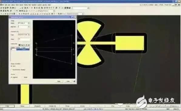
The circuit board in the original, the 68pin module on the left is an rfid module, the position A of the red dot is the pin that outputs the rf signal, the pins on both sides of the pin are ground; the right side of the picture is a design designed by TI. Standard inverted F antenna for the rf chip. The red dot position B is the feed point.
This photo is a prototype made by a foreign school. It is possible to connect point A and point B directly. It seems that it should work. My question is:
Is the connection between the two points of A/B very strict in terms of length, line width, distance between rf copper and GND? Still almost on the line? Our application is rfid application, the signal requirements may not be as strict as the mobile phone, but we do not want people to design the module 80m distance, it can only transmit 20 meters on our board, it is too ugly.
Detailed explanation of 2.4G wireless technology
Section 1: Advantages of 2.4G wireless technology
The so-called 2.4G wireless technology, the frequency band is between 2.405GHz-2.485GHz (science, medicine, agriculture). So referred to as 2.4G wireless technology. This band is an internationally stipulated free frequency band and does not require any payment to international organizations. This provides the necessary advantages for the development of 2.4G wireless technology. Moreover, 2.4G wireless technology is different from the previous 27MHz wireless technology. Its working mode is full-duplex mode transmission, which has an absolute advantage in anti-interference performance than 27MHz. This advantage determines its superior immunity to interference and transmission distances of up to 10 meters. In addition, 2.4G wireless technology also has a theoretical 2M data transmission rate, which is twice the theoretical transmission rate of Bluetooth. This will improve the reliability of the future application layer. Combining the four commonly used wireless transmission technologies of 2.4G, Bluetooth and 27MHz, 2.4G has its own unique advantages. Compared to Bluetooth, its products are cheaper to manufacture and offer higher data transfer rates. Compared to the same free 27MHz wireless technology, its anti-interference, maximum transmission distance and power consumption are far beyond.
2.4G wireless mouse
The 2.4G wireless mouse and keyboard set has been around for a while, and it has been steadily occupying the market for low-end wireless mouse and keyboard. Bluetooth is still being used as a high-end wireless technology on mouse and keyboard. Market share is relatively small but indispensable because Bluetooth has its own relatively open connection protocol. Rather than the point-to-point connection of 2.4G wireless through the code. However, because the identity of the mouse and the mouse is quite special, a set of keyboard and mouse for a computer is enough. Unlike a PSP or a mobile phone, it is a carrier that can use Bluetooth's point-to-point function to send and receive data. This determines the future development trend of 2.4G wireless technology in mouse and keyboard products.
2.4G wireless keyboard
既然是未æ¥çš„å‘展趋势,被用户广泛应用是时间迟早的问题。讲究便æºã€æŠ—干扰ã€ä»¥åŠä¼ 输è·ç¦»çš„HTPC用户æ°å¥½å’Œ2.4Gæ— çº¿æŠ€æœ¯çš„è¯¸å¤šç‰¹ç‚¹ç›¸èžåˆã€‚如今很多知åçš„é”®é¼ åŽ‚å•†å·²ç»æŠŠæœªæ¥çš„æ— çº¿æŠ€æœ¯äº§å“å‘展方å‘对准了2.4G。有了大的厂商带动,相信越æ¥è¶Šå¤šçš„用户会对2.4Gæ— çº¿é”®é¼ äº§å“产生浓厚的兴趣。
2.4Gæ— çº¿é”®é¼ æ”¶å‘模å—介ç»
通过我们一直以æ¥å¯¹å¸‚场ä¸å¤§éƒ¨åˆ†å“牌的资料收集,基本目å‰å¸‚场ä¸çš„2.4Gæ— çº¿é”®é¼ äº§å“æ‰€ç”¨åˆ°çš„æ— çº¿æ”¶å‘模å—都是NRF24L01芯片,æ¤æ¬¾èŠ¯ç‰‡å‡ºè‡ªæŒªå¨è‘—åIC芯片公å¸Nordic。
The utility model relates to a medical atomization treatment and humidifying device belonging to the technical field of medical equipment and household appliances.
Professional Medical Atomization manufacturer is located in China, including Medical Vape,Dose Control Vape Pen,Supersonic Wave Vape, etc.
Medical Atomization,Medical Vape,Dose Control Vape Pen,Supersonic Wave Vape
Shenzhen MASON VAP Technology Co., Ltd. , https://www.cbdvapefactory.com