
Feature:
1. Proviging 7-14 hours Lighting time, and USB phone charger solution
2. can choose 3, 4lamps option
3. easy installation and easy to use
4. 1 year warranty and Over 3years Lifespan
5. Solar home kit, Light Up 2 rooms at the same time
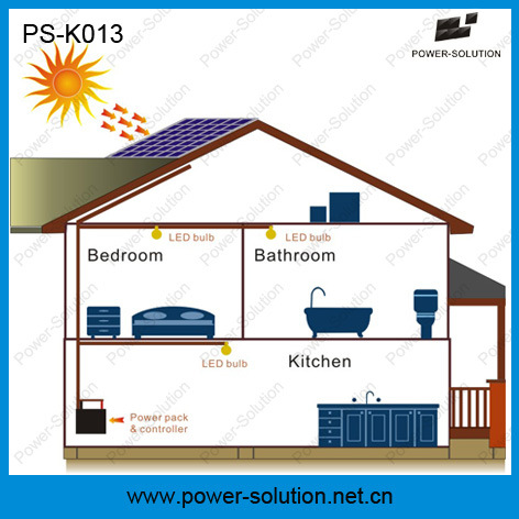
Solar Lighting Kit for Rural Family Daily Lighting and Phone Charger Solution
1. Installation—all-in-one DIY kitÂ
2. Cable—with on\off switchÂ
3. Mobile phone charge—for different phonesÂ
4. Power supply—solar or AC adapter
5. Protection—overcharge and over-discharge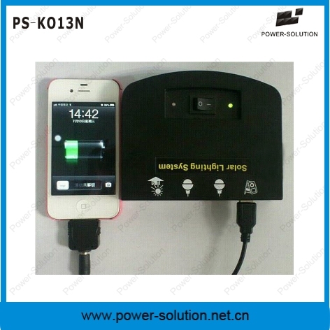
Professional  Manufacturer (Factory Pictures)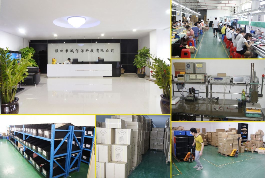
Our Company Website:Â
Alibaba.com: Â http://power-solution.en.alibaba.com
   Â
Globalmarket:Â Â http://power-solution.gmc.globalmarket.com
Official Website:Â www.power-solution.net.cn
Contact Us:
Sales: Â Shawn Dong
Phone:+86-13714107880
Â
Standard PCB
A Printed Circuit Board (PCB) mechanically supports and electrically connects electronic components using conductive tracks, pads and other features etched from copper sheets laminated onto a non-conductive substrate. Components (e.g. capacitors, resistors or active devices) are generally soldered on the PCB. Advanced PCBs may contain components embedded in the substrate.
PCBs can be single sided (one copper layer), double sided (two copper layers) or multi-layer (outer and inner layers). Conductors on different layers are connected with vias. Multi-layer PCBs allow for much higher component density.
FR-4 glass epoxy is the primary insulating substrate. A basic building block of the PCB is an FR-4 panel with a thin layer of copper foil laminated to one or both sides. In multi-layer boards multiple layers of material are laminated together.
Printed Circuit Boards are used in all but the simplest electronic products. Alternatives to PCBs include wire wrap and point-to-point construction. PCBs require the additional design effort to lay out the circuit, but manufacturing and assembly can be automated. Manufacturing circuits with PCBs is cheaper and faster than with other wiring methods as components are mounted and wired with one single part.
Here at BentePCB, Standard PCB means manufacture parameter in General requirements, no special features.
Parameter Definition of Standard PCB as below:
|
Items |
Manufacturing Capabilities |
|
Number of Layers |
1-16 layers |
|
Material |
FR-4 |
|
Maximum PCB Size(Dimension) |
650x1200 mm |
|
Board Size Tolerance(Outline) |
±0.2mm/±0.5mm |
|
Board Thickness |
0.8-1.6mm |
|
Board Thickness Tolerance(t≥1.0mm) |
±10% |
|
Board Thickness Tolerance(t<1.0mm) |
±0.1mm |
|
Min Trace |
0.1mm/4mil |
|
Min Spacing |
|
|
Copper Thickness |
1oz(35μm) |
|
Drill Sizes (CNC) |
0.3-6.3mm |
|
Min Width of Annular Ring |
0.15mm(6mil) |
|
Finished Hole Diameter (CNC) |
0.3mm-6.2mm |
|
Finished Hole Size Tolerance(CNC) |
±0.08mm |
|
Solder Mask |
LPI |
|
Minimum Character Width(Legend) |
0.15mm |
|
Minimum Character Height (Legend) |
0.8mm |
|
Character Width to Height Ratio (Legend) |
1:05 |
|
Minimum Diameter of Plated Half Holes |
0.6mm |
|
Surface Finishing |
HASL with lead |
|
Solder Mask |
HASL lead free |
|
Immersion gold |
|
|
Green ,Red, Yellow, Blue, White ,Black |
|
|
Silkscreen |
White, Black, None |
|
Panelization |
V-scoring, |
|
|
Tab-routing, |
|
Tab-routing with Perforation (Stamp Holes) |
|
|
|
About Us:
BentePCB is a professional PCB manufacturing which is focus on double side, multilayer, HDI PCB , rigid PCB and Flexible PCB mass production. The company was established on 2011.
We have two factories together, The factory in Shenzhen is specialized in small and middle volume orders and the factory in Jiangxi is for big volume.
Why Us?
UL (E492586), ISO9001, ISO14001, TS16949, RoHS certified.
Turnover USD 10-50 million per year.
15,000 sqm area, 450 staff .
Mass Production from single to 16 layers.
Special Material:ROGERS, Arlon, Taconic.etc.
Client:Huawei, SAMSUNG, Malata, Midea,Texas Instruments.etc.
Certification(UL:E492586, TS16949, ISO14001, ISO9001,RoHS):


Factory Tour:


Exhibition:
We Took part in the famous exhibitions over the past years,and got highly appreciation from the top experts,as well as cooperated tightly with them.

Delivery:
BentePCB offers flexible shipping methods for our customers, you may choose from one of the methods below.


We don`t just sell PCBs .We sell sleep.

Standard PCB
Standard PCB, Printed Circuit Board, Circuit Board, PCB Circuit Board
Shenzhen Bente Circuit Limited , http://www.bentegroup.com