
Embedded DDR (Double Data Rate) design is the most important and core part of embedded hardware design with DDR. As the processing capability of embedded systems becomes more and more powerful, more and more functions are implemented, and the operating frequency of the system is getting higher and higher, the operating frequency of DDR is gradually increased from the lowest 133 MHz to 200 MHz, thereby realizing even more. Big system bandwidth and better performance. However, the higher operating frequency also imposes higher requirements on the stability of the system. This requires hardware designers to have more constraints and considerations on the layout of the circuit. The most important part that can affect whether the whole system works normally and is stable is the circuit design of the DDR part. The embedded system uses DDR memory and can achieve better performance on traditional single data rate memory chips..
1 DDR bus structureFor DDR memory, JEDEC established and adopted a low-voltage, high-speed signal standard. This standard is called "StubSeries Terminated Logic (SSTL)." The SSTL can improve the signal integrity of data transmitted over the bus. The purpose of this terminal design is to prevent data corruption due to signal reflections at high speeds.
In a typical memory topology, if a series termination resistor (Rs) is used, it should be placed away from the DDR controller. This approach saves valuable board space near the controller, avoids cabling congestion and cumbersome fanout; it also optimizes the signal integrity from the controller to the memory chip, often with many address and command signals in these locations. Need to be reliably received by multiple memories.
The most common SSTL terminal model is a better single terminal and parallel terminal scheme, as shown in Figure 1. This scheme involves using a series termination resistor (Rg) from the controller to memory, and a shunt termination resistor (RT) pulled up to the termination voltage (VTT). This method is common on motherboards of commercial computers, but current embedded motherboards are often used for better signal integrity and system stability. The value of Rs and RT is dependent on the specific system and the board-level simulation should be used to determine the specific value.

Transmission of high-speed bus signals often requires consideration of signal integrity issues. The signal line of the DDR is not an ordinary signal line but a transmission line. Therefore, the via holes on the transmission line, or the discontinuous impedance factors such as the connector, all affect the signal integrity at the receiving end. There are overshoots and undershoots, ringing, and crosstalk effects. Some inaccuracies in AC noise and DC voltage also affect signal transmission performance.
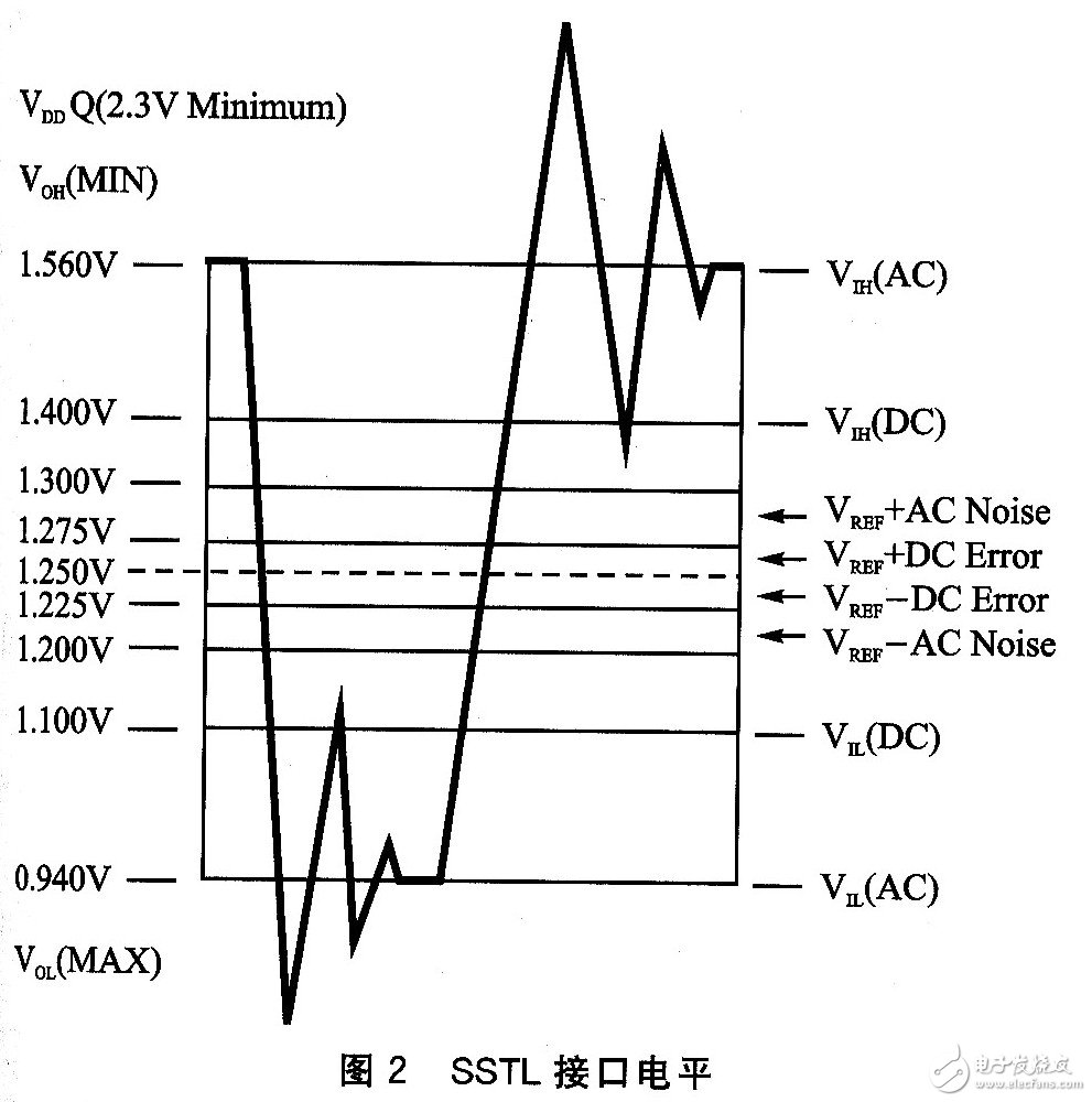
DDR To achieve a higher signal frequency, the received level of the SSTL high-gain differential receiver is often biased near the reference level (VREF), using such a receiver allows a smaller voltage swing, less signal reflection , lower electromagnetic interference and shorter settling time, can adapt to higher clock frequency than LVTTL. Figure 2 shows the SSTL interface level. The AC logic level is the receiver level at the receiver, where the AC logic parameters (including setup and hold times) must be optimal at the receiver, and the DC logic level provides a lagging reception level point. When the input level passes through the DC DC reference point, the receiver transitions to a new logic level and maintains this new state as long as the signal is not below the threshold level. Therefore, the SSTL bus is not susceptible to overshoot, undershoot, and ringing.
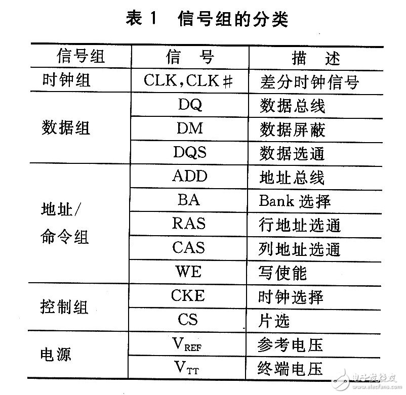
The DDR controller includes more than 130 signals and provides a direct signal interface to the memory subsystem. These signals can be divided into different signal groups according to the type of signal, as listed in Table 1. Among them, the data group should be divided into each byte channel, DMO, DQSO and DQO ~ DQ7 for the first byte of the channel, DMl, DQSl and DQ8 ~ DQl5 for the second byte of the channel, and so on. There is a strict length matching relationship within each byte lane. The length of other signal traces should be matched in units of groups. The difference in signal length in each group should be strictly controlled within a certain range. Although the signals of different groups are not as stringent as the intra-group signals, the differences in lengths of different groups also have certain requirements. For detailed wiring requirements, see section 2.4.
To ensure that the DDR interface is optimized, the DDR routing should be performed in the following order: power, pin swapping in a resistive network, data signal line routing, address/command signal routing, control signal routing, clock signal routing, and feedback signal routing.
The routing priority of the data signal group is the highest among all signal groups because it operates at twice the clock frequency and its signal integrity requirements are the highest. In addition, the data signal group is the portion of the memory bus that occupies the largest part of all these signal groups, and the most important signal length group matches the required signal group.
Address, command, control, and data signal groups are all related to the clock traces. Therefore, the effective clock trace length in the system should satisfy multiple relationships. Designers should establish a comprehensive consideration of system timing to ensure that all these relationships are met.
2.4 Matching Signal Wiring Length of Each GroupClock signal: referenced to the ground plane to provide a complete ground plane for the entire clock loop trace, providing a low impedance path to the loop current. Because it is a differential clock signal, the line width should be designed in advance before wiring, and the differential impedance is calculated. Then, the wiring is performed according to this constraint. All DDR differential clock signals must be routed on the critical plane to avoid layer-to-layer transitions. The line width and differential spacing need to refer to the DDR controller's implementation details. The single line impedance of the signal line should be controlled at 50-60Ω and the differential impedance controlled at 100-120 Ω. Clock signals to other signals should be kept at a distance of 20 mil* or more to prevent interference with other signals. The serpentine trace spacing should not be less than 20 mils. The series termination resistor Rs is in the range of 15 to 33Q, and the optional parallel termination resistor RT is in the range of 25 to 68 Ω. The specific resistance value should be based on the signal integrity simulation result.
Data signal group: reference to the ground plane to provide a complete ground plane for the signal loop. The characteristic impedance is controlled at 50~60 Ω. Line width requirements refer to the implementation rules. Is at least 20 mils away from other non-DDR signals. The length matching is set in units of byte channels. The length difference of the data signal DQ, data strobe DQS and data mask signal DM in each byte channel should be controlled within ~25 mil (very important), and the signal length of different byte channels. The difference should be controlled within 1 000 mi. Match the matching DM and DQS series matching electrical Rs values ​​from o to 33 Ω, parallel matching termination resistors RT values ​​from 25 to 68 other DDR signals.
Address and command signal groups: Keep the ground and power planes intact. The characteristic impedance is controlled at 50 to 60 Ω. The signal line width refers to the specific design implementation details. The distance between signal groups and other non-DDR signals should be at least 20 mils. The in-group signal should match the DDR clock line length, with a gap of at least 25 mils. The series matching resistor Rs is 0~33 Ω and the parallel matching resistor T should be 25~68 Ω. The signals in this group should not be in the same resistor row as the data signals.
Control signal group: The control signal group has the least signal, only the clock enable and chip select two signals. Still need a complete ground plane and power plane for reference. The series matching resistor RS is O~33 Ω, and the parallel matching termination resistor RT is 25~68 Ω. In order to prevent crosstalk, the signals in this group also cannot be in the same resistor row as the data signals.
2.5 Design Analysis of Power Supply SectionUnder normal circumstances, the DDR supply voltage is 2.3 to 2.7 V, and the typical value is 2.5 V. Different operating frequencies may cause different operating voltages. The reference voltage VREF is 1.13 to 1.38 V, and the typical value is 1.25 V. VTT is referenced to VREF, and the voltage range is (VREF-O.4 V)-(VREF+O·4 V). Since VREF only supplies a DC reference level to the differential receiver, the current is relatively small. The maximum is only 3mA. VTT current is due to pull-up. When the output is high, VTT should be able to sink current at the output. Output VTT current output when low power. Therefore, VTT must be able to have both inflow and outflow of current, the size of the current depends on the potential state of the bus at the same time, from the common design point of view can be from 2.3A to 3.2A.
Since the VREF voltage is an important reference for other signal receivers, its wiring design is also very important. Crosstalk or noise superimposed on the VREF voltage can directly cause potential timing errors, jitter, and drift on the memory bus. Many power chips will output VREF and VTT from the same source, but the traces are completely different due to different purposes. VREF is preferably in a different plane than VTT to avoid VTT-generated noise interfering with VREF. In addition, no matter the DDR controller or DDR memory, decoupling capacitors should be placed near the VREF pin to eliminate high-frequency noise. The width of the VREF trace should be as wide as possible, preferably 20 to 25 mils.
The VTT power supply should be divided into a single plane to supply current, and it is best to put it on the DDR memory side. If the parallel terminations match the pull-up method, it is best to add a 0.1 μF or 0·01 μF decoupling capacitor for each of the resistors. This improves the integrity of the signal and improves the stability of the DDR bus. Have a good effect.
ConclusionIn embedded system boards with DDR, the most difficult part of designing a PCB is the DDR trace design. A good trace is equivalent to good signal integrity and good timing matching. The bus will not go wrong during high-speed input/output data and can even have better crosstalk and EMC immunity. The DDR bus transmits in parallel and has a relatively high speed. If the wiring is not performed according to strict constraints during the design process, various abnormal problems will occur during the device's later debugging process, and even the system cannot be started at all. These problems are hard to find in finding and debugging, so that it is impossible to complete the hardware development. The best way is to fully consider the issue of signal integrity and timing matching in designing. Apply these rules when wiring. If there are conditions, you can do some simulation and verify the design in advance. With this design, the stability and reliability of the system will be even higher.
Suizhou simi intelligent technology development co., LTD , https://www.msmvape.com